Semiconductor device stress modeling methodology

Inactive Publication Date: 2008-08-14
GLOBALFOUNDRIES INC
View PDF13 Cites 55 Cited by
  • Summary
  • Abstract
  • Description
  • Claims
  • Application Information

AI Technical Summary

Benefits of technology

[0059]The semiconductor circuit may comprise a MOSFET and the re-fitted stress model may employ a first scalar, which is a longitudinal channel stress, and a second scalar, which is a transverse channel stress, wherein the effect of a three-dimensional stress field

Problems solved by technology

Stress impacts the performance of semiconductor devices by altering the band structure of the semiconductor material, and consequently, the mobility of carriers.
However, channel length scaling may not be self-consistent because the base model inadvertently includes a component of channel length scaling introduced by the le

Method used


Image

  • Semiconductor device stress modeling methodology
  • Semiconductor device stress modeling methodology
  • Semiconductor device stress modeling methodology

Examples


Embodiment Construction

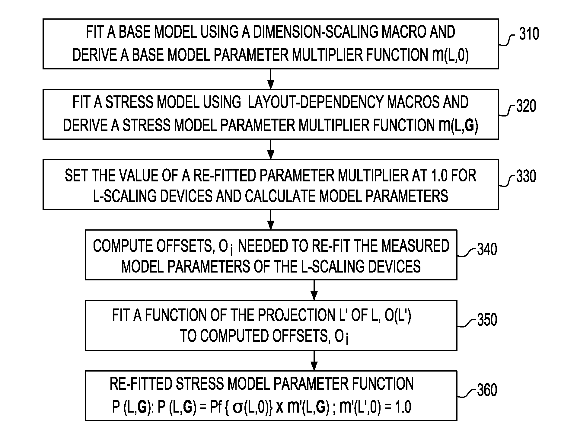
[0070]As stated above, the present invention relates to a methodology for determining device model parameters that are affected by layout-dependent stress, including metal-oxide-transistor field effect transistor (MOSFET) carrier mobility and threshold voltage, to a system for modeling the stress-dependent device characteristics of semiconductor devices, to a system for simulating semiconductor circuits affected by stress, and to a system for optimizing semiconductor circuits that are affected by stress, which are now described in detail with accompanying figures.

[0071]The stress-dependent model parameter P may be any model parameter in a compact model that is altered by applied stress and characterizes device characteristics. The stress-dependent model parameter P is calculated from the layout-dependent information of a semiconductor device, or from the semiconductor circuit data typically in the format of a netlist, which may be extracted from a layout data set through an extracti...


PUM


Abstract

A computational methodology that improves the accuracy of model parameters in a compact model uses methods and algorithms to self-consistently match independently developed base and stress models by re-fitting the stress model to the data set that generates the base model. The re-fitting algorithm removes any discrepancy between the base model and the stress model as the stress model is applied to the data set obtained from a dimension-scaling macro. Stress offsets for dimension-scaling macro devices are calculated to fit the measured values of the model parameters for the same devices. The process of fitting the model parameters to the data set from the dimension-scaling macro calculates constant, linear, and quadratic coefficients for the model parameters, which are employed to increase the accuracy of the model parameters and of the compact model used in circuit simulations and optimization.

Description

FIELD OF THE INVENTION[0001]The present invention relates to a methodology for determining stress-dependent semiconductor device model parameters for semiconductor devices and, more particularly, to a methodology for determining device model parameters that are affected by layout-dependent stress, including metal-oxide-transistor field effect transistors (MOSFETs) carrier mobility and threshold voltage, and to a system for modeling the stress-dependent device characteristics of semiconductor devices, and to a system for simulating semiconductor circuits affected by stress, and to a system for optimizing design of semiconductor circuits that are affected by stress.BACKGROUND OF THE INVENTION[0002]Accurate modeling of semiconductor devices is needed to provide reliable circuit simulation results that can predict the behavior of a semiconductor circuit. Often, circuit simulations are used during a design phase of a circuit to predict circuit characteristics such as the drive current of...

Claims


Application Information

Patent Timeline
IPC IPC(8): G06F17/50
CPCG06F17/5009G06F2217/16G06F17/5068G06F2111/10G06F30/39G06F30/20G06F30/398
Inventor CHIDAMBARRAO, DURESETIWILLIAMS, RICHARD Q.
Owner GLOBALFOUNDRIES INC
Why Eureka
Try Eureka