Substrate Processing Apparatus

a processing apparatus and substrate technology, applied in the direction of manufacturing tools, grinding machine components, edge grinding machines, etc., can solve the problems of dust management of particles, inability of conventional inspection units to perform measurement of wafer shape, and inability to perform operation management in polishing units

Active Publication Date: 2008-08-21
EBARA CORP
View PDF7 Cites 55 Cited by
  • Summary
  • Abstract
  • Description
  • Claims
  • Application Information

AI Technical Summary

Benefits of technology

[0009]The present invention has been made in view of the above drawbacks. It is, therefore, a first object of the present invention to provide a substrate processing apparatus which can polish a peripheral portion of a substrate and measure the peripheral portion of the substrate.

Problems solved by technology

One of, the major problems in managing particles is dust caused by surface roughness produced at a peripheral portion (a bevel portion and an edge portion) of a substrate, such as a semiconductor wafer, in a manufacturing process of semiconductor devices.
The conventional inspection unit cannot perform measurement of a shape of a wafer, such as a cross-sectional shape of the peripheral portion of the wafer or a radius of the wafer.
Thus, operation management has not been performed in the polishing unit.
Further, the conventional inspection unit is expensive because it performs a high degree of image processing with use of an imaging device such as a CCD camera and an image processing device.
Further, a long period of time is required for inspection because of image processing.
Thus, the polishing process becomes complicated so as to lower the process efficiency.
Further, if the inspection results show insufficiency of removal of defects or contaminants at the peripheral portion of the wafer in the polishing unit, it is necessary to return the wafer to the polishing unit and polish the peripheral portion of the wafer again.
In such a case, the polishing process cannot be performed speedily.

Method used


Image

  • Substrate Processing Apparatus
  • Substrate Processing Apparatus
  • Substrate Processing Apparatus

Examples


fourth embodiment

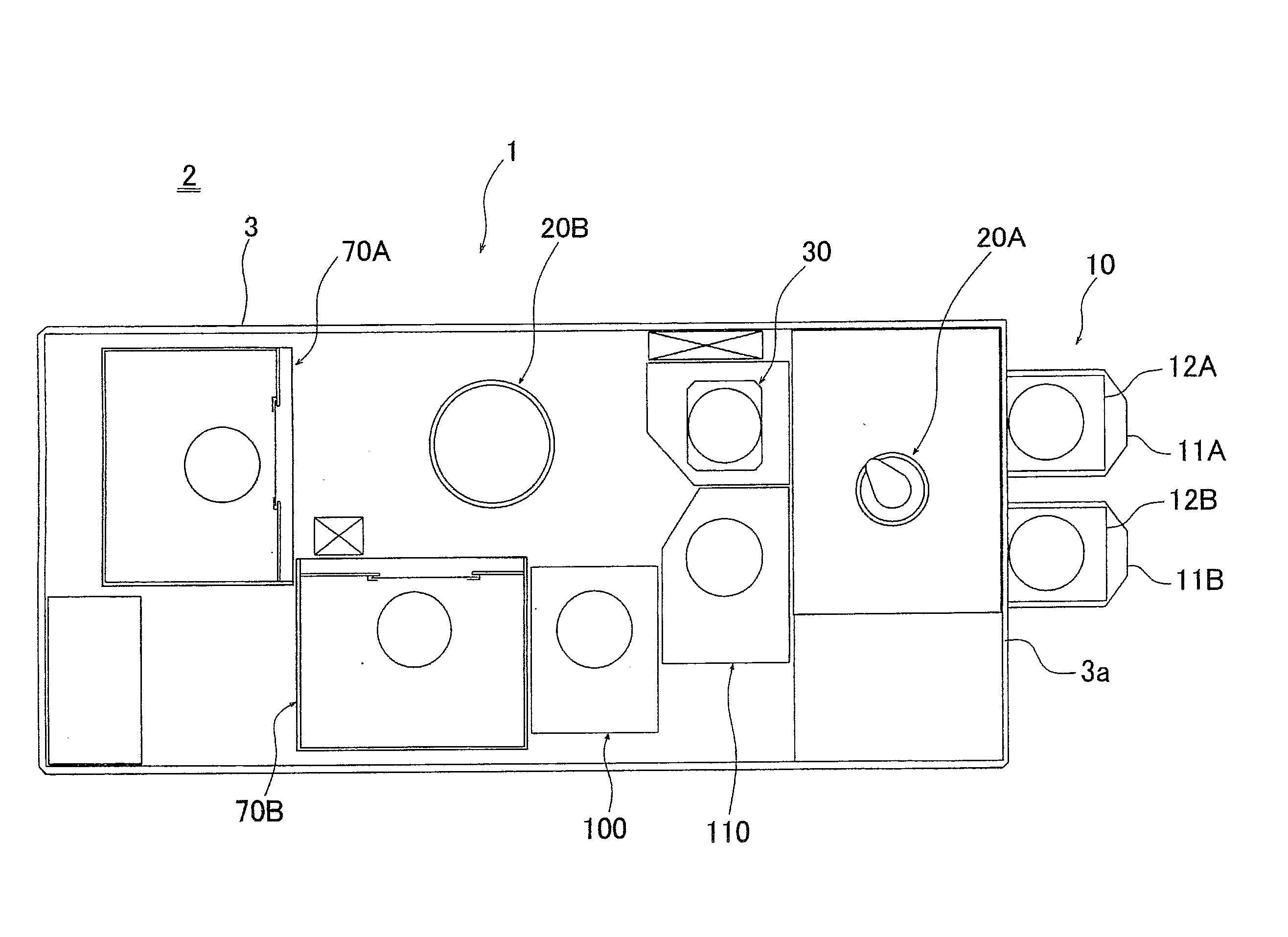
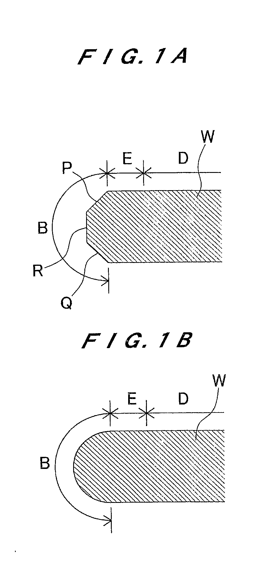
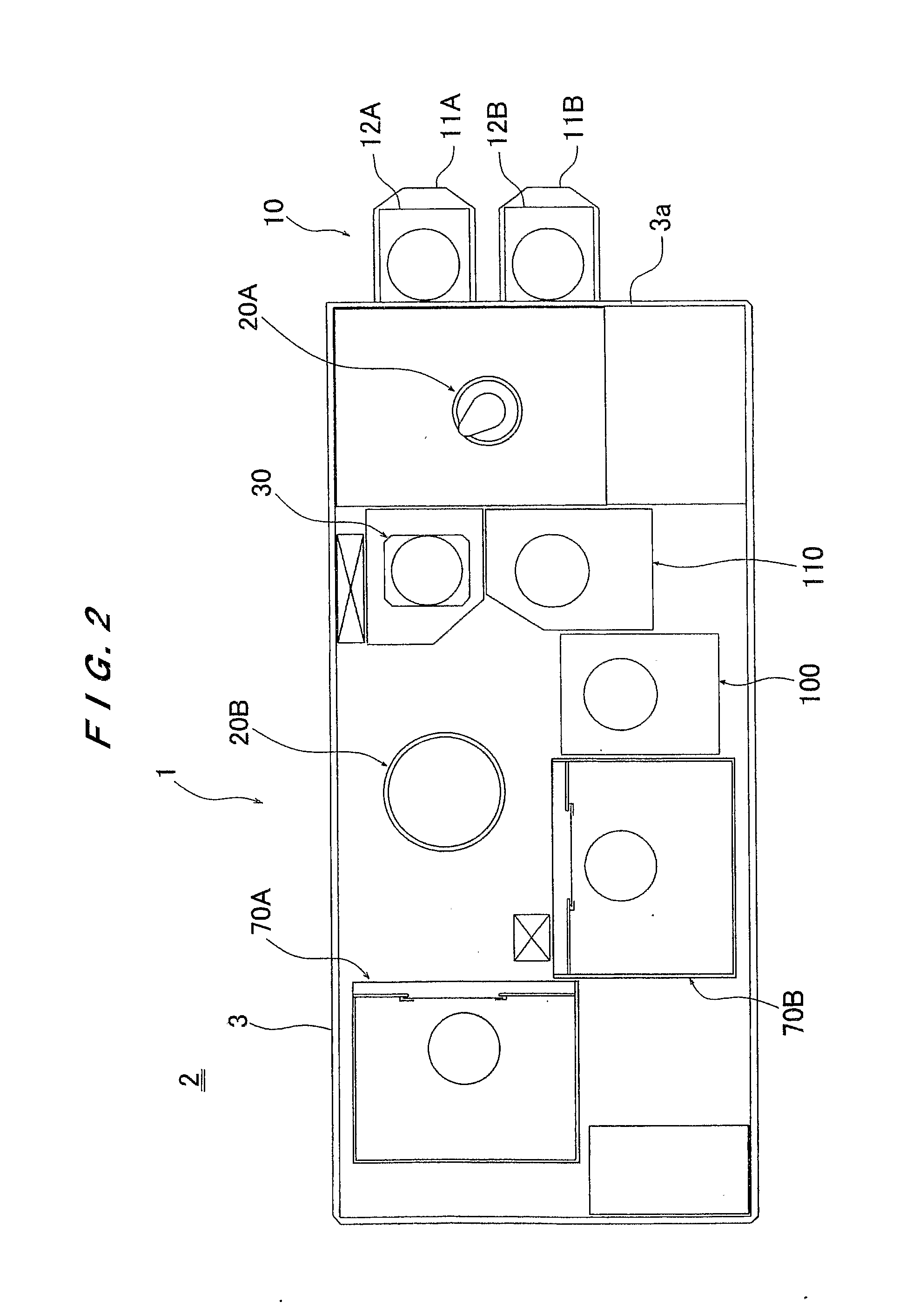
[0151]In the following example, a wafer is polished under polishing conditions which are determined based on measurement results in the measurement unit 30 having the cross-sectional shape measurement mechanism, such as the measurement unit 30-2, 30-3, or 30-4 in the second, third, or FIG. 27 shows a cross-sectional shape of a peripheral portion of a wafer W. Polishing conditions including polishing angles M1 and M2 of an upper inclined portion P and a lower inclined portion Q and a polishing angle M3 of a side surface R of a bevel portion of the wafer W are determined based on measured data of the wafer W which are measured in the measurement unit 30 with the cross-sectional shape measurement mechanism before polishing. Further, an expected polishing amount is calculated from the cross-sectional shape of the wafer W and polishing conditions including pressing forces of the polishing surface and rotational speeds of the wafer in the polishing unit 70A or 70B. Thus, a polished shape...

fifth embodiment

[0154]The measurement unit 30 having the surface condition measurement mechanism, such as the measurement unit 30-5 in the fifth embodiment, can measure surface conditions of a peripheral portion of a polished wafer and inspect status of removal of objects attached to the peripheral portion of the wafer in the polishing unit 70A or 70B or removal of surface roughness. When a polished wafer is thus measured, it is possible to determine whether or not desired polishing has been conducted in the polishing unit 70A or 70B. Accordingly, operation of the polishing unit 70A or 70B can be managed at an optimal state.

[0155]In the case where a polished wafer is measured in the measurement unit 30, the measure wafer is returned from the measurement unit 30 to the wafer cassette 12A or 12B. Thus, all wafers in the wafer cassette 12A or 12B are processed in the substrate processing apparatus 1 and returned to the wafer cassette 12A or 12B. Then, if it is determined from the inspection results of...


PUM

PropertyMeasurementUnit
average particle diameteraaaaaaaaaa
polishing angleaaaaaaaaaa

Abstract

A substrate processing apparatus (1) includes first and second polishing units (70A, 70B) for polishing a peripheral portion of a substrate (W), a primary cleaning unit (100) for cleaning the substrate (W), a secondary cleaning and drying unit (110) for drying the substrate (W) cleaned in the primary cleaning unit (100), and a measurement unit (30) for measuring the peripheral portion of the substrate (W). The measurement unit (30) includes a mechanism for measurement required for polishing in the first and second polishing units (70A and 70B), such as a diameter measurement mechanism, a cross-sectional shape measurement mechanism, or a surface condition measurement mechanism.

Description

TECHNICAL FIELD[0001]The present invention relates to a substrate processing apparatus, and more particularly to a substrate processing apparatus having a polishing unit for polishing a peripheral portion of a substrate such as a semiconductor wafer. The present invention also relates a substrate processing method, and more particularly to a substrate polishing method of polishing a peripheral portion of a substrate such as a semiconductor wafer. The present invention is also concerned with a substrate measuring method of measuring a peripheral portion of a substrate such as a semiconductor wafer.BACKGROUND ART[0002]In recent years, according to finer structures and higher integration of semiconductor devices, it has become more important to manage particles. One of, the major problems in managing particles is dust caused by surface roughness produced at a peripheral portion (a bevel portion and an edge portion) of a substrate, such as a semiconductor wafer, in a manufacturing proce...

Claims


Application Information

Patent Timeline
Patent Type & Authority Applications(United States)
IPC IPC(8): B24B9/06H01L21/304B24B49/12
CPCB24B9/065B24B49/04H01L21/68728H01L21/67253H01L21/68707H01L21/67219H01L21/304H01L21/302H01L21/461
Inventor TAKAHASHI, TAMAMISHIRAKASHI, MITSUHIKOITO, KENYAINOUE, KAZUYUKIYAMAGUCHI, KENJISEKI, MASAYA
Owner EBARA CORP
Why Eureka
Try Eureka