Eureka AIR delivers breakthrough ideas for toughest innovation challenges, trusted by R&D personnel around the world.

Solid state imaging device and imaging apparatus

Inactive Publication Date: 2008-08-28
SONY CORP
View PDF1 Cites 6 Cited by
  • Summary
  • Abstract
  • Description
  • Claims
  • Application Information

AI Technical Summary

Benefits of technology

[0021]It is also desirable to prevent color mixture, to achieve a higher sensitivity, and to scale the pixel size down.
[0023]In the solid state imaging device according to the embodiment of the invention, since the second well region is formed in the area except the place corresponding to the photosensor part, the color mixture can be prevented even though the pixel size is scaled down. In addition, the dependency of sensitivity and spectral response on the voltage Vsub to apply can be improved. In other words, since the second well region exists at a position deeper than the first well region, even though the voltage Vsub is increased, the position of the minimum value of potential is in the first well region and is not shifted to the position near the photosensor part. Thus, a higher sensitivity can be implemented as well as an improved dependency of sensitivity and spectral response on the voltage Vsub to apply can be implemented. Accordingly, even though the pixel size is scaled down, the color mixture can be prevented, and a higher sensitivity can be implemented as well as an improved dependency of sensitivity and spectral response on the voltage Vsub to apply can be implemented.
[0025]In the imaging apparatus according to the embodiment of the invention, the solid state imaging device according to the embodiment of the invention is used for the imaging device. Thus, even though the pixel size is scaled down, the color mixture can be prevented, and a higher sensitivity can be implemented as well as an improved dependency of sensitivity and spectral response on the voltage Vsub to apply can be intended.
[0026]In accordance with the solid state imaging device according to the embodiment of the invention, even though the pixel size is scaled down, the color mixture can be prevented, and a higher sensitivity can be implemented as well as an improved dependency of sensitivity and spectral response on the voltage Vsub to apply can be intended. Therefore, such advantages are provided that a higher definition and a higher image quality of taken images are possible.
[0027]In accordance with the imaging apparatus according to the embodiment of the invention, even though the pixel size of the solid state imaging device used for the imaging device is scaled down, the color mixture can be prevented, and a higher sensitivity can be implemented as well as an improved dependency of sensitivity and spectral response on the voltage Vsub to apply can be intended. Thus, such advantages are provided that a higher definition and a higher image quality of taken images are possible.

Problems solved by technology

In the case of this structure, since a voltage drop occurs in the place apart from the ground part, holes are delayed to migrate in the photosensor, and overflow barrier potential on the route B fluctuates in the surrounding area and the center part of an effective imaging area to cause shading in saturated signal electrons, which leads to degraded image quality of a taken image.
However, in this case, it is difficult to empty the overflow barrier area because the overflow barrier area is neutralized, which leads to a problem of blooming when a large light quantity enters.
However, this causes a problem that the resistance in the overflow barrier area is increased to cause shading when a large light quantity enters.
On this account, in the structure of the channel stop areas formed only on the surface of a semiconductor substrate, it is difficult to efficiently prevent a phenomenon that photoelectrically converted electric charges are mixed into the adjacent pixels in the photosensor part (hereinafter, referred to as color mixture).
However, in the case of using this method, the impurity concentration becomes nonuniform in the depth direction, and it is difficult to form a channel stop area of uniform impurity concentration to a deeper area.
Therefore, in the case in which the pixel size is small, it is difficult to form the overflow barrier area to a position deep from the substrate surface.
However, as described above, in the case in which the pixel size is small, it is difficult to form the overflow barrier area at a deep position, which leads to a problem that it is difficult to allow a solid state imaging device to have higher sensitivity.
Moreover, when the channel stop area becomes nonuniform in the depth direction, the potential becomes wavy in the depth direction, which is not preferable to drain excess holes out of the channel stop area to the front surface side of the substrate.
The problem of difficulty of higher sensitivity and the problem of a nonuniform channel stop area become particularly problematic when the pixel size is 2 μm or below.
In addition, the method described in Patent Reference 2 has a problem that the number of process steps is increased.
Moreover, it is necessary to form a thicker ion injection mask formed of a resist because it is necessary to form the channel stop part by high energy ion implantation, which causes a difficulty of microprocessing a thick resist film, also leading to a problem that it is difficult to form pixels finer.
Therefore, in this case, it is difficult to attain the prevention of color mixture as well as a higher sensitivity.
Thus, in the case in which the method described in Patent Reference 2 is adapted to the invention described in Patent Reference 1, there is a problem that it is difficult to scale the pixel size down.

Method used


Image

  • Solid state imaging device and imaging apparatus
  • Solid state imaging device and imaging apparatus
  • Solid state imaging device and imaging apparatus

Examples


first embodiment

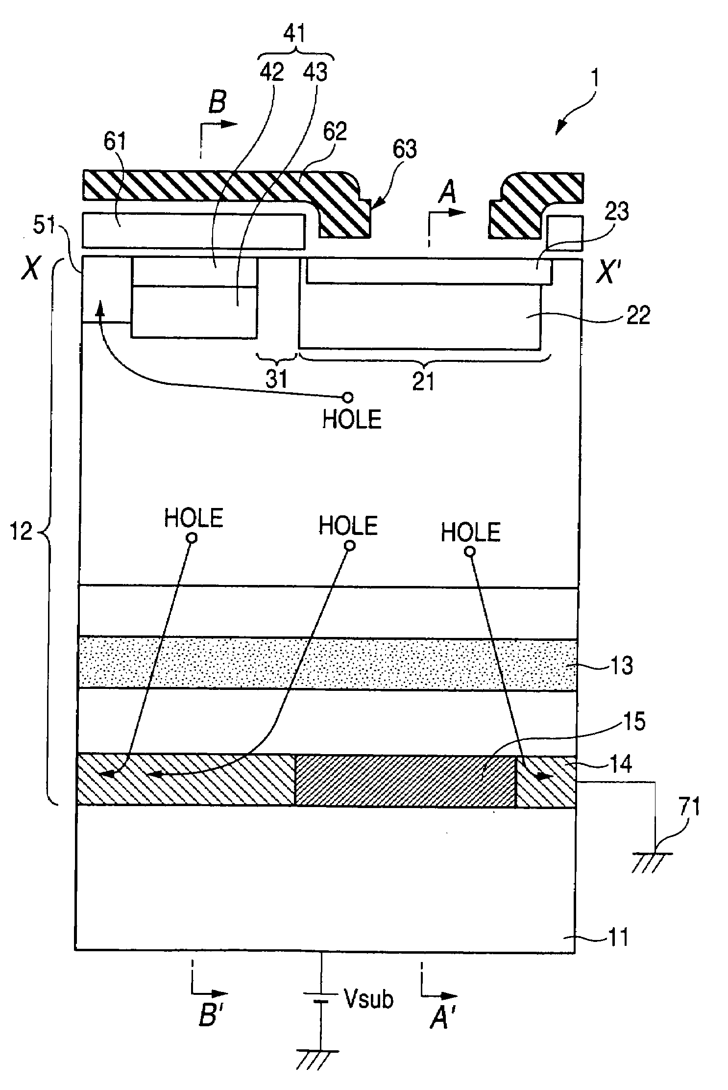
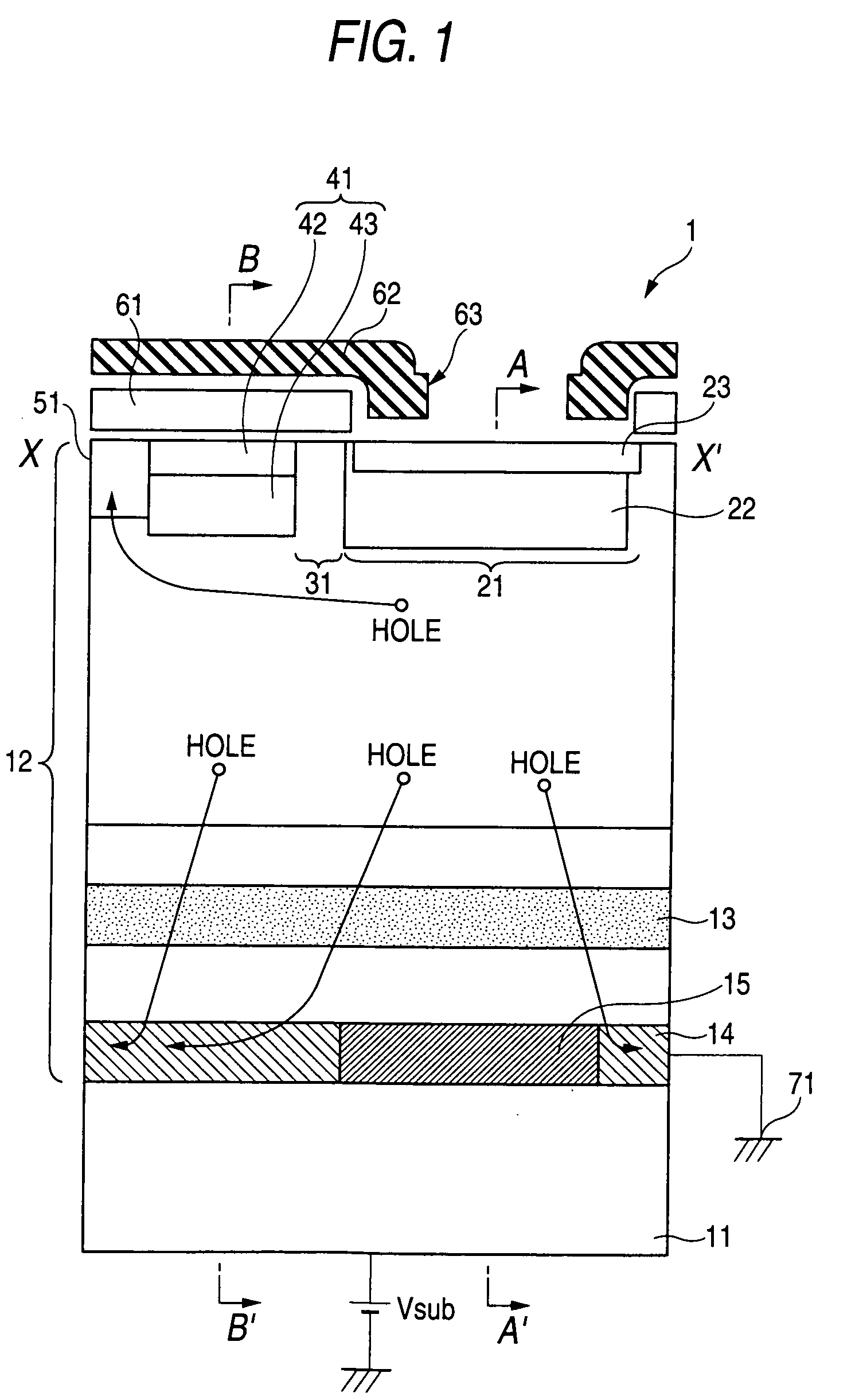
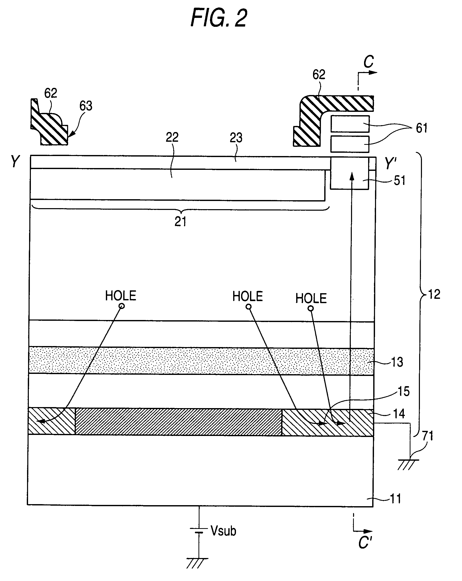
[0037]A solid state imaging device according to an embodiment (first embodiment) of the invention will be described with reference to cross sections shown in FIGS. 1, 2 and 3 and plan layout diagrams shown in FIGS. 4 and 5. Moreover, FIG. 1 shows a diagram depicting an X-X′ schematic cross section in FIG. 4, and FIG. 2 shows a diagram depicting a Y-Y′ schematic cross section in FIG. 4.

[0038]In addition, FIGS. 1, 2, and 4 show a diagram schematically depicting the vicinity of a single light receiving pixel among a plurality of light receiving pixels provided in an image area of a solid state imaging device according to the embodiment of the invention. FIG. 3 shows a cross section depicting the schematic configuration of the vicinity of a ground part provided on the outer part of the image area of the solid state imaging device according to the embodiment of the invention. FIG. 5 shows a layout diagram schematically depicting the image area of the solid state imaging device and the vi...

second embodiment

[0073]Next, a solid state imaging device according to the invention will be described with reference to a cross section depicting the schematic configuration shown in FIG. 8.

[0074]As shown in FIG. 8, a solid state imaging device 2 is provided with a first conductive type (N-type) area 18 between the second well region 14 and the semiconductor substrate 11 in the solid state imaging device 1, the area 18 that has a concentration high enough to cancel the striation of a silicon substrate. Preferably, the concentration of the first conductive type region 18 (the concentration of the N-type impurity such as As or P) is about 2.0×1016 cm−3 to 5.0×1017 cm−3. For example, the first conductive type region 18 is formed in which an N-type impurity is ion injected into the semiconductor substrate 11. Although it is necessary to form the first conductive type region 18 at a deep position 6 μm or deeper from the surface of the light receiving area 23, it is difficult to form the area at a deep p...


PUM


Abstract

A solid state imaging device having an image area in which a plurality of light receiving pixels is arranged on a semiconductor substrate of a first conductive type is disclosed. The device includes: a plurality of photosensor parts formed by providing on the semiconductor substrate a light receiving area and a photoelectric conversion area both configuring the light receiving pixel; a first well region formed on the opposite side of the light receiving area, having a second conductive type opposite to the first conductive type, and forming an overflow barrier; a second well region of the second conductive type formed in an area except a place corresponding to the photosensor part on the opposite side of the photoelectric conversion area; and a first conductive region formed in an area corresponding to the photosensor part on the opposite side of the photoelectric conversion area.

Description

CROSS REFERENCES TO RELATED APPLICATIONS[0001]The present invention contains subject matter related to Japanese Patent Application JP 2007-044447 filed in the Japanese Patent Office on Feb. 23, 2007, the entire contents of which being incorporated herein by reference.BACKGROUND OF THE INVENTION[0002]1. Field of the Invention[0003]The present invention relates to a solid state imaging device and an imaging apparatus.[0004]2. Description of the Related Art[0005]Heretofore, a so-called vertical overflow drain solid state imaging device is proposed in which excess electrons in a light receiving part are drained to the substrate side and excess holes are evacuated to a ground part (GND) from a channel stop part provided around individual photosensors on the substrate surface through a P-type region disposed at a deep place in the substrate.[0006]Moreover, a structure is disclosed in which excess holes are partially drained to GND out of a channel stop part around individual photosensors ...

Claims


Application Information

Patent Timeline
IPC IPC(8): H01L27/00H01L27/148H04N5/335H04N5/359H04N5/369H04N5/372
CPCH01L27/14887H01L27/146
Inventor HARADA, KOUICHI
Owner SONY CORP
Why Eureka
Eureka Blog
Learn More