Semiconductor white light emitting device and method for manufacturing the same

Inactive Publication Date: 2008-09-04
ROHM CO LTD
View PDF0 Cites 199 Cited by
  • Summary
  • Abstract
  • Description
  • Claims
  • Application Information

AI Technical Summary

Benefits of technology

[0014]According to the present invention, the semiconductor light emitting element includes the green and blue light emitting layers which have ratios of In smaller than that of a light emitting layer capable of emitting red light, so that both the light emitting layer

Problems solved by technology

However, increasing the ratio of In in the InGaN layer reduces the crystallinity and reduces the emission intensity of red light to below a desired emission intensity.
However, it is difficult to control the ratios of the t

Method used


Image

  • Semiconductor white light emitting device and method for manufacturing the same
  • Semiconductor white light emitting device and method for manufacturing the same
  • Semiconductor white light emitting device and method for manufacturing the same

Examples


first embodiment

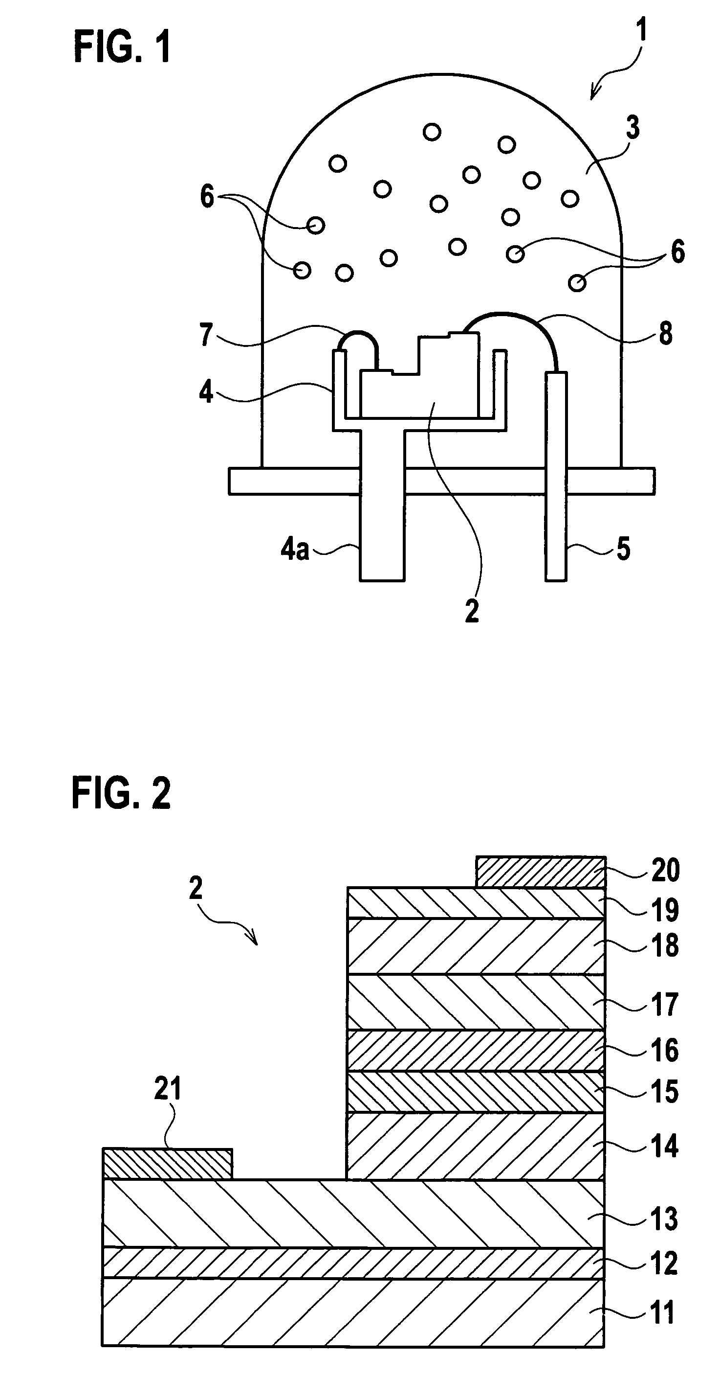
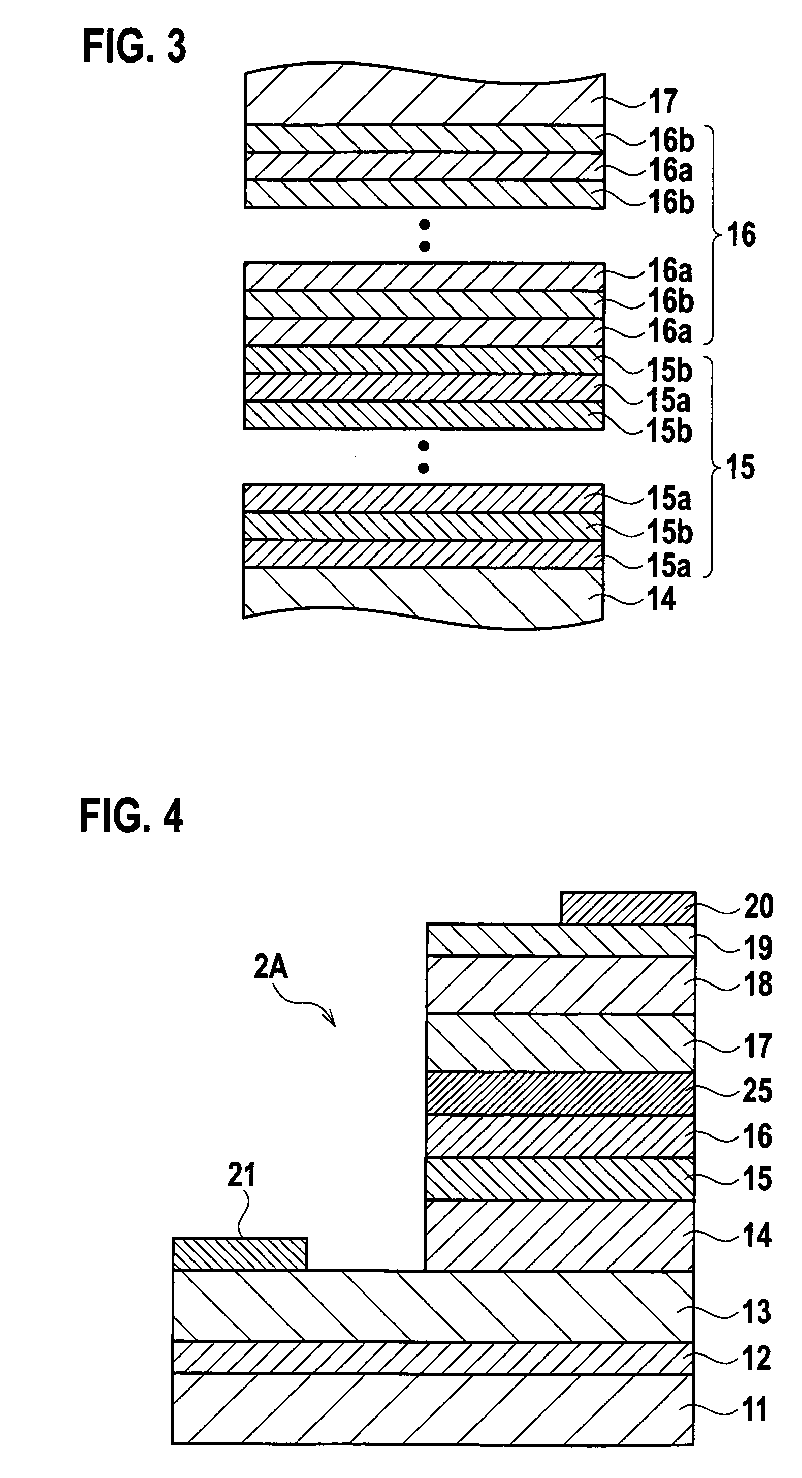
[0022]With reference to the drawings, a description is given below of a first embodiment of the present invention. FIG. 1 is a schematic view of a semiconductor white light emitting device according to the first embodiment of the present invention. FIG. 2 is a cross-sectional view of a semiconductor light emitting element, and FIG. 3 is a cross-sectional view of light emitting layers of the semiconductor light emitting element.

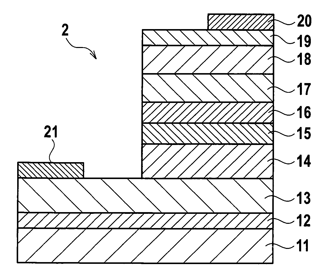
[0023]As shown in FIG. 1, the semiconductor white light emitting device 1 includes a semiconductor light emitting element 2, a package 3, a supporting member 4, and an external terminal 5.

[0024]As shown in FIG. 2, the semiconductor light emitting element 2 includes a buffer layer 12, an n-type contact layer 13, an n-type clad layer 14, a green light emitting layer 15, a blue light emitting layer 16, a p-type clad layer 17, a p-type contact layer 18, and a transparent electrode 19, which are sequentially stacked on a sapphire substrate 11. The semiconductor lig...

second embodiment

[0055]Next, with reference to the drawings, a description is given of a semiconductor white light emitting device according to a second embodiment obtained by partially modifying the semiconductor light emitting element of the semiconductor white light emitting device of the first embodiment. FIG. 4 is a cross-sectional view of the semiconductor light emitting element according to the second embodiment. Similar components to those of the first embodiments are given same reference numerals.

[0056]As shown in FIG. 4, the semiconductor light emitting element 2A includes an ultraviolet light emitting layer 25 formed between the blue light emitting layer 16 and p-type clad layer 17. The ultraviolet light emitting layer 25 emits ultraviolet light (wavelength: about 100 to 430 nm). The ultraviolet light emitting layer 25 has an MQW structure in which eight pairs of alternating well and barrier layers (not shown) are stacked cyclically. Each of the well layers is composed of an about 3 nm th...


PUM


Abstract

A semiconductor white light emitting device including: a semiconductor light emitting element having green and blue light emitting layers containing In; and a phosphor capable of emitting red light.

Description

CROSS REFERENCE TO RELATED APPLICATIONS AND INCORPORATION BY REFERENCE[0001]This application is based upon and claims the benefit of priority from prior Japanese Patent Application P2006-328285 filed on Dec. 5, 2006; the entire contents of which are incorporated by reference herein.BACKGROUND OF THE INVENTION[0002]1. Field of the Invention[0003]The present invention relates to a semiconductor white light emitting device including a semiconductor light emitting element having a plurality of light emitting layers capable of emitting light of different colors.[0004]2. Description of the Related Art[0005]A known conventional semiconductor white light emitting device includes a semiconductor light emitting element having a plurality of light emitting layers emitting light of different colors.[0006]For example, Japanese Patent Laid-open Publication No. 2005-217386 (Patent Literature 1) discloses a first semiconductor white light emitting element including: a semiconductor light emitting d...

Claims


Application Information

Patent Timeline
IPC IPC(8): H01L33/00H01L33/20H01L33/08H01L33/32H01L33/50H01L33/56H01L33/62
CPCH01L33/08H01L33/50H01L2224/49107H01L2224/48091H01L2224/48247H01L2224/48257H01L2924/00014
Inventor SENDA, KAZUHIKONAKATA, SHUNJI
Owner ROHM CO LTD
Why Eureka
Try Eureka