
Liquid crystal display device and plasma display device

Inactive Publication Date: 2008-09-04
HITACHI LTD +2
View PDF13 Cites 7 Cited by
  • Summary
  • Abstract
  • Description
  • Claims
  • Application Information

AI Technical Summary

Benefits of technology

[0012]1): Providing a transparent substrate as a front plate on the outermost surface to improve breakage resistance.
[0013]2): Filling the gap between a polarizing plate and the transparent substrate and removing an air layer to reduce interfacial reflection.
[0094]The breakage resistance is improved by providing the front plate on the image display panel. Also, it has been shown that the reflectance on the air interface is reduced in comparison with a case where no organic medium is provided.

Problems solved by technology

On the other hand, with the spreading of liquid crystal television sets in ordinary home use, there have been increasing cases of using liquid crystal television displays in homes where pets such as cats and dogs live or in homes where infants live and, hence, increasing cases of the television screen being broken by being struck by an object or by being beaten.
A plasma television display is of a structure using a thick front plate and not easily breakable but has such a large distance from the image formation surface to the outermost surface of the front plate that a displayed image is blurred and obscure if an antiglare layer is used in the outermost surface.
Plasma television displays therefore use antireflection film in ordinary cases but are incapable of completely reducing specular reflection and have considerable glare or external image reflection.
Moreover, in manufacture of a liquid crystal panel, since the two glass plates between which a liquid crystal is sealed in has a small thickness of 0.5 to 0.7 mm, there is a risk of the glass being broken if the liquid crystal panel is held with an unnecessarily large force in each conveyance step in manufacturing or at the time of wiring for example.
However, if an air layer exists between the image display surface and the front plate, the transmittance is reduced or double reflection is caused due to interfacial reflection, resulting in a reduction in visibility.
The antireflection film is incapable of completely reducing specular reflection and there is a limit to the reduction of external image reflection.

Method used


Image

  • Liquid crystal display device and plasma display device
  • Liquid crystal display device and plasma display device
  • Liquid crystal display device and plasma display device

Examples


example 1

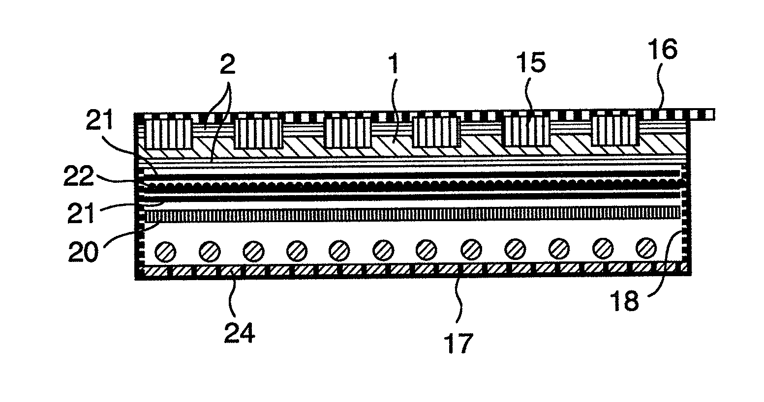
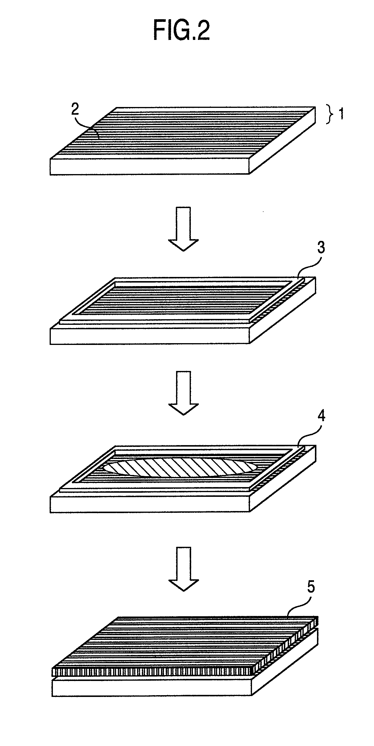
[0231]Two liquid crystal modules were made. Each liquid crystal module was of a construction such that a liquid crystal panel to which two polarizing plates were attached was provided on the light emitting side of a backlight. A 1.8 mm thick glass plate was provided as a front plate on one of these liquid crystal modules, with polyisobutylene interposed therebetween as a transparent organic medium. An antiglare-processed film of 3% haze was attached to the surface of the front plate on the light emitting side. The thickness of the polyisobutylene was about 1 mm. The same glass plate was provided on the other liquid crystal module with an air layer interposed therebetween, without filling the gap with polyisobutylene. An antiglare-processed film of 3% haze was attached to the surface of the front plate on the light emitting side.

[0232]A comparison was made between the modules with the front plates to find that stronger surface reflection appears on the module not filled with polyisob...

example 2

[0237]Two liquid crystal modules were made. Each liquid crystal module was of a construction such that a liquid crystal panel to which two polarizing plates were attached was provided on the light emitting side of a backlight are made. A control system, a power supply and other components were mounted on each of the two liquid crystal modules, thereby making image display devices. Also, LCD control driver ICs were mounted on a lower portion of each liquid crystal module. A 2 mm thick glass plate was provided as a front plate on one of these liquid crystal display devices, with polyisobutylene interposed therebetween as a transparent organic medium. The thickness of the polyisobutylene was about 1 mm.

[0238]A weak alkaline glass cleaner was sprayed to remove dust on the screen, and the screen was thereafter wiped with a cloth. Then a portion of the screen of the image display device on which no front plate was provided stopped displaying an image. No such a phenomenon occurred in the ...

example 3

[0240]A liquid crystal module was made which was the same as the liquid crystal module using the transparent organic medium in Example 1 except that an acrylic resin containing 0.1 wt % of a pigment NK3981 (a product from Hayashibara Biochemical Labs., Inc.) in place of polyisobutylene was provided as the transparent organic medium between the polarizing plate and the front plate.

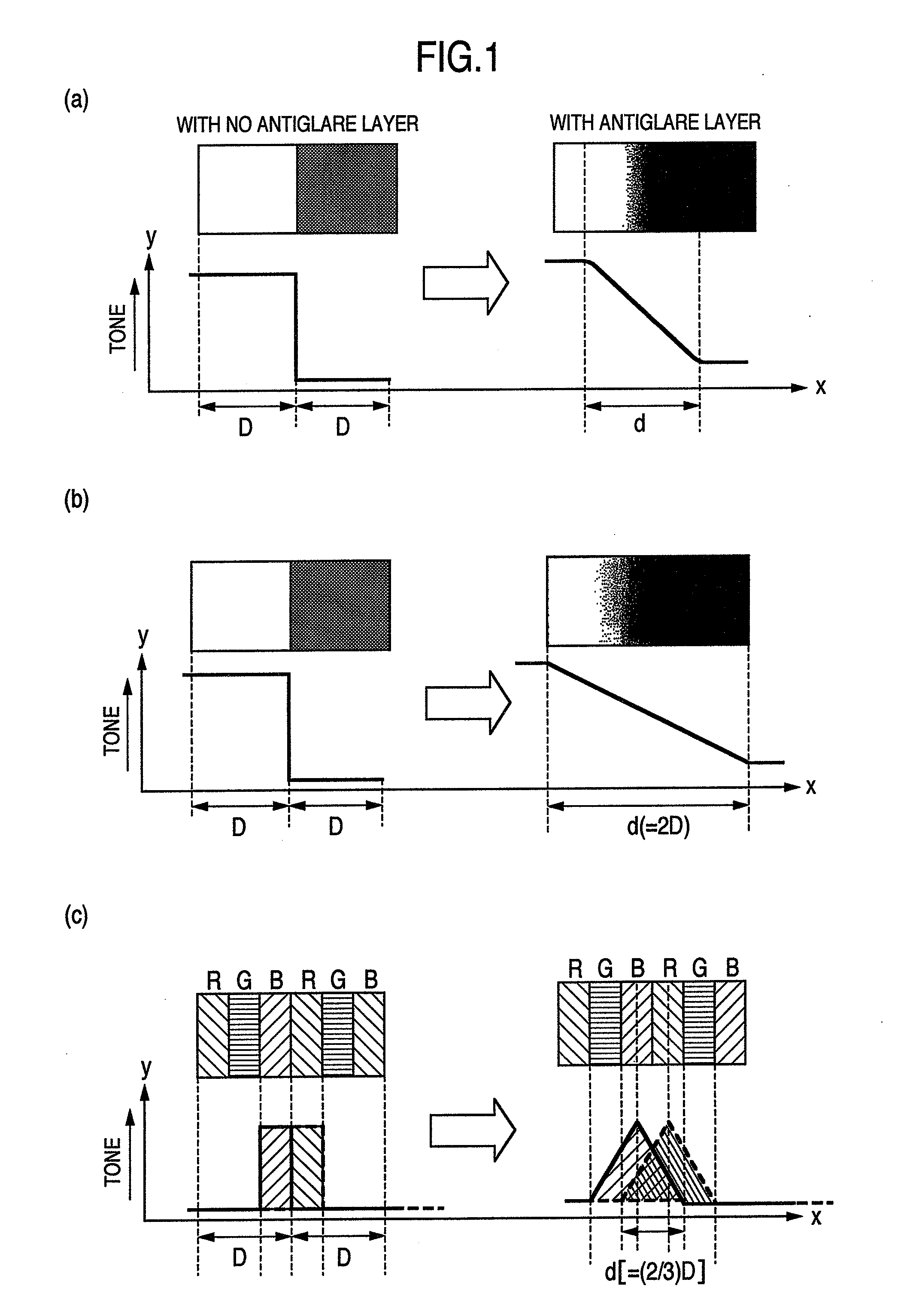
[0241]In the constitution according to this example, the transparent organic medium functions as a spectral absorption layer having an absorption peak at a wavelength of about 490 nm due to the effect of the mixed pigment. From this, it can be expected that a leakage of light with a wavelength of about 490 nm caused by scattering through the color filter is absorbed to achieve an increase in contrast ratio.

[0242]A color filter used in a liquid crystal panel has blue, green and red colored layers formed by using organic pigments. For example, PB15:6+PV23 for blue, PG36+PY150 for green and PR177+PY83 for red ...


PUM


Abstract

An image display device designed to improve shock resistance and to eliminate external image reflection and blurring. In an liquid crystal display device are disposed a backlight, a polarizing plate on the backlight side and a liquid crystal panel held by two glass substrates and having electrodes, a liquid crystal layer, an alignment layer and a color filter therein. The image display device has a transparent front plate provided on the liquid crystal panel opposite from the backlight, a transparent organic medium layer provided between the front plate and the liquid crystal panel, and an antiglare layer provided on the front plate opposite from the transparent organic medium layer.

Description

BACKGROUND OF THE INVENTION [0001]The present invention relates to a liquid crystal display device and a plasma display device. More particularly, the present invention relates to a liquid crystal display device or a plasma display device having a transparent front plate on the image display screen.[0002]In an image display device using a liquid crystal, light from a light source is caused to pass through certain members such as a liquid crystal layer interposed between thin glass plates, a color filter and a polarizing plate to be recognized as an image. The outermost surface of such a display device for use as a personal computer monitor or a liquid crystal television display is a polarizing plate. To reduce reflection on the interface between the polarizing plate surface and an air layer, fine irregularities are formed on the polarizing plate surface or an antiglare layer containing particles is formed on the polarizing plate surface.[0003]On the other hand, with the spreading of...

Claims


Application Information

Patent Timeline
IPC IPC(8): G02F1/13357G02F1/1335G02F1/1333H01J17/49G09F9/00H01J11/44
CPCG02F1/133502H01J11/44G02F2202/02
Inventor SUGIBAYASHI, MAKIKOSASAKI, HIROSHIKONDO, KATSUMINAKAMURA, KIYOMITOMIOKA, YASUSHI
Owner HITACHI LTD
Features
  • Generate Ideas
  • Intellectual Property
  • Life Sciences
  • Materials
  • Tech Scout
  • Unparalleled Data Quality
  • Higher Quality Content
  • 60% Fewer Hallucinations
Learn More