Memory unit structure and operation method thereof
a memory unit and operation method technology, applied in the field of memory unit structure, can solve the problems of affecting the operation, cycle endurance and data retention of the memory unit, affecting the performance of the swing, etc., and achieve the effect of stabilizing the swing performan
- Summary
- Abstract
- Description
- Claims
- Application Information
AI Technical Summary
Benefits of technology
Problems solved by technology
Method used
Image
Examples
first embodiment
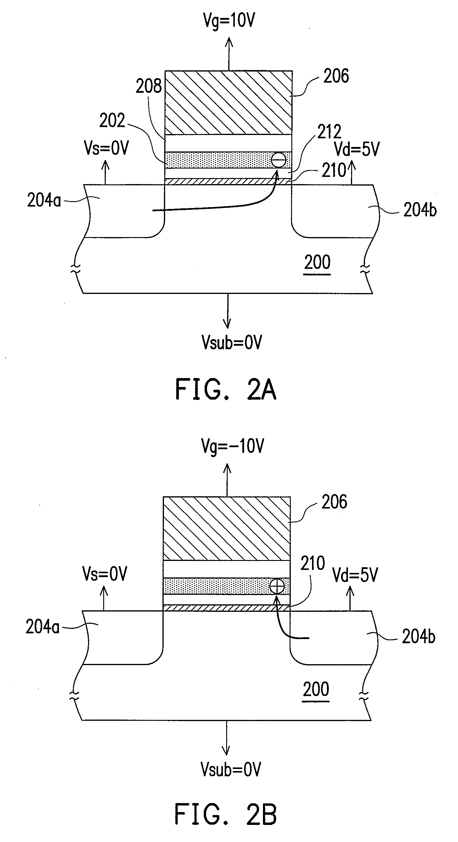
[0049]FIG. 2A is a cross-section view of a memory unit structure according to the invention during a two-bit programming operation.
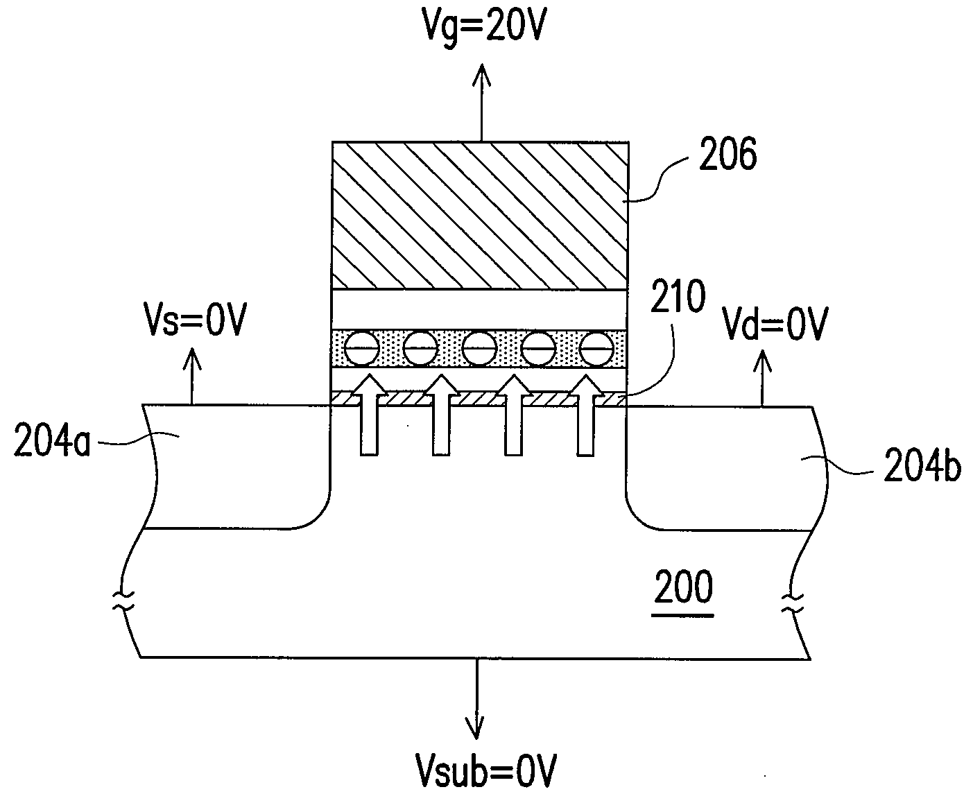
[0050]Referring to FIG. 2A, the memory unit of the first embodiment includes a Si substrate 200, a trapping layer 202, a first doping region 204a and a second doping region 204b, a gate 206, a first oxide layer 208, a high-Dit material layer 210 and a second oxide layer 212. In this embodiment, the Si substrate 200 is a p-type Si substrate, and the first doping region 204a and the second doping region 204b are n-type doping regions. The trapping layer 202 is on the Si substrate 200, and the first and the second doping regions 204a and 204b are formed in the Si substrate 200 on either side of the trapping layer 202, respectively. The gate 206 is formed on the trapping layer 202, and the first oxide layer 208 is formed between the gate 206 and the trapping layer 202. The high-Dit material layer 210 is formed between the Si substrate 200 and the trapping la...
second embodiment
[0059]FIG. 4A is a cross-section view of a memory unit structure according to the invention during a two-bit programming operation.
[0060]Referring to FIG. 4A, the memory unit of the second embodiment includes a Si substrate 400, a trapping layer 402, a first doping region 404a and a second doping region 404b; a gate 406, a first dielectric layer 408 and a second dielectric layer 410. In this embodiment, the Si substrate 400 is a p-type Si substrate, the first and the second doping regions 404a, 404b are n-type doping regions, wherein the first dielectric layer 408 is an oxide layer, for example. There is an interface 412 having high interface trap (HIT) property between the second dielectric layer 410 and the Si substrate 400, the interface trap density (Dit) of which is in the range of 1011 cm−2eV−1 to 1013 cm−2eV−1, preferably 1012 cm−2eV−1. Furthermore, the second dielectric layer 410 can be an oxide layer. For example, a worst thermal oxidation process or an implantation method ...
PUM
 Abstract
Description
Claims
Application Information


