

Chip carrier structure having semiconductor chip embedded therein and metal layer formed thereon
- Summary
- Abstract
- Description
- Claims
- Application Information
AI Technical Summary
Benefits of technology
Problems solved by technology
Method used
Image

Examples
first embodiment
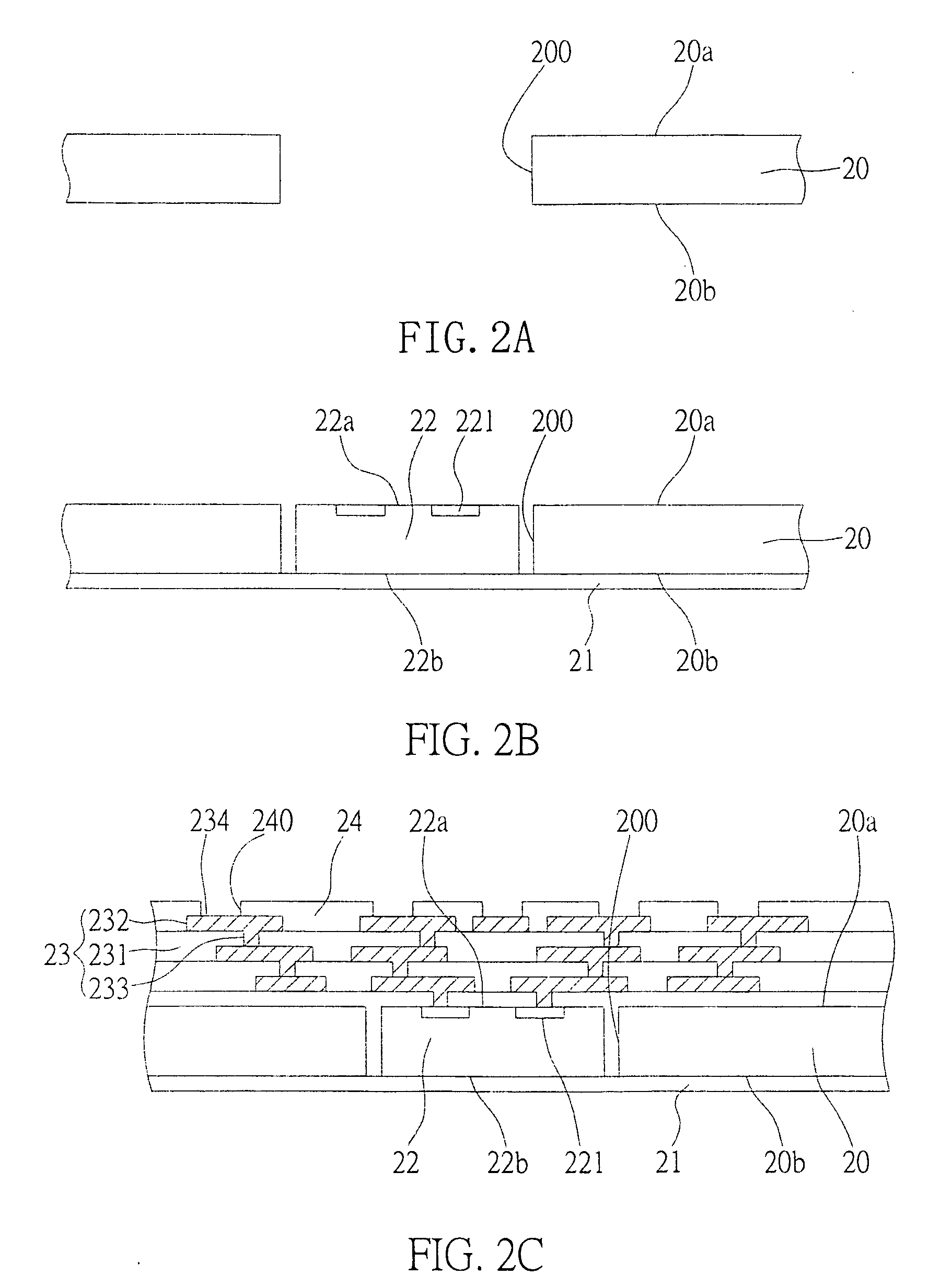
[0030]Referring to FIGS. 2A to 2H, cross-sectional schematic views of a chip carrier structure having a semiconductor chip embedded therein and a protective metal layer formed thereon according to the first embodiment of the present invention are shown.
[0031]In FIG. 2A, a carrier board 20 having a first surface 20a and a second surface 20b is first provided. The carrier board 20 has at least one opening 200 penetrating the first and second surfaces 20a and 20b. The carrier board 20 can, for example, be one of a circuit board, insulated board and metal board.
[0032]Referring to FIG. 2B, a release film 21 is formed on the second surface 20b of the carrier board 20 to seal one end of the opening 200. A semiconductor chip 22 is then attached on the release film 21 within the opening 200. The semiconductor chip 22 has an active surface 22a formed with a plurality of electrode pads 221 and an inactive surface 22b.
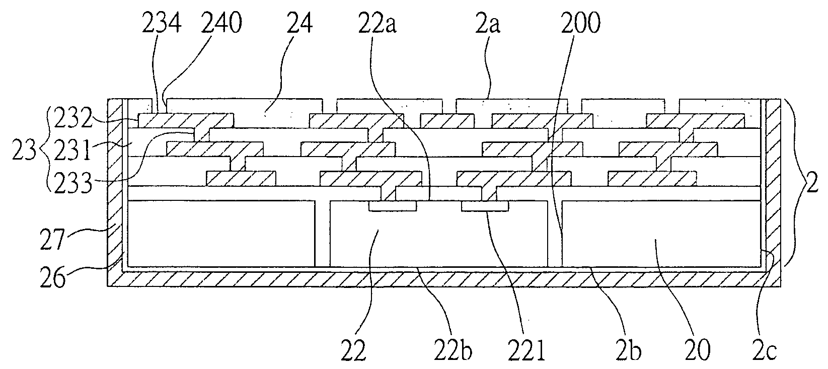
[0033]Referring to FIG. 2C, a circuit build up structure 23 is formed on the...
second embodiment
[0044]Referring to FIGS. 3A to 3C, which illustrate the second embodiment of the present invention. The second embodiment is different from the first embodiment in that an opening 267 is further formed in the metal layer 27 and the conductive layer 26 at the bottom of the chip carrier 2 embedded with a semiconductor chip, to expose the inactive surface 22b of the semiconductor chip 22, and facilitate heat dissipation by directly exposing the inactive surface 22b.
[0045]Referring to FIG. 3A, a structure shown in FIG. 2F is provided. A resist layer 28 is formed on the surface of the conductive layer 26. Resist openings 280 are formed in the resist layer 28 to expose the bottom surface 2b and the side surfaces 2c of the chip carrier 2 but cover the inactive surface 22b of the semiconductor chip 22.
[0046]As shown in FIG. 3B, an electroplating process is performed to form a metal layer 27 on the surface of the conductive layer 26 that is within the resist opening 280.
[0047]As shown in FI...
PUM
 Abstract
Description
Claims
Application Information