Interconnect for an electrical circuit substrate

Inactive Publication Date: 2008-09-11
DELPHI TECH INC
View PDF6 Cites 10 Cited by
  • Summary
  • Abstract
  • Description
  • Claims
  • Application Information

AI Technical Summary

Benefits of technology

[0007]In an embodiment, the present invention provides a low profile attachment of substrates, wherein the substrates are attached forming a planar structure. Space is conserved on a printed circuit board since the present invention interconnect can be utilized as a functional passive component, beyond being a simple interconnect. In one case, signal transmission from the first substrate to the second substrate is routed via the present invention interconnect. Passive components normally occupying space can be utilized as the interconnect and are relocated closer to a component thereby increasing electrical performance.
[0008]In an alternative embodiment, a standoff is created between the first substrate and the second substrate to set the two substrates apart a desired distance. The standoff defined between the two substrates can be utilized for a structure such

Problems solved by technology

PGAs and small-outline integrated circuit (SOIC), or dual-in-line surface mount packages, were being produced with an increasing number of pins, and with decreasing spacing between the pins, causing difficulties for the soldering process.
As package pins got closer together, the danger of accidentally bridging adjacent pins with solder grew.
A disadvantage of BGAs,

Method used


Image

  • Interconnect for an electrical circuit substrate
  • Interconnect for an electrical circuit substrate
  • Interconnect for an electrical circuit substrate

Examples


Example

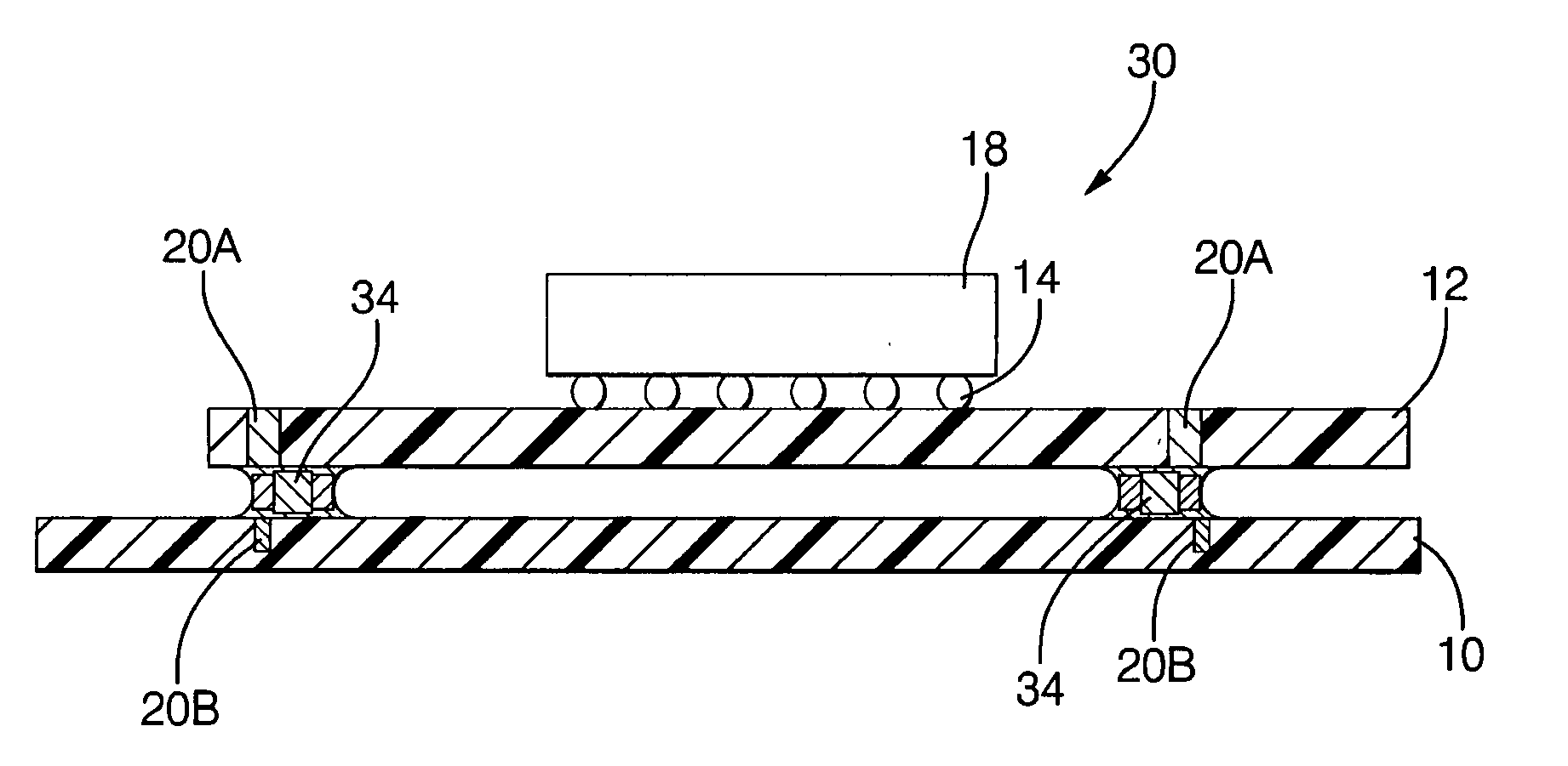
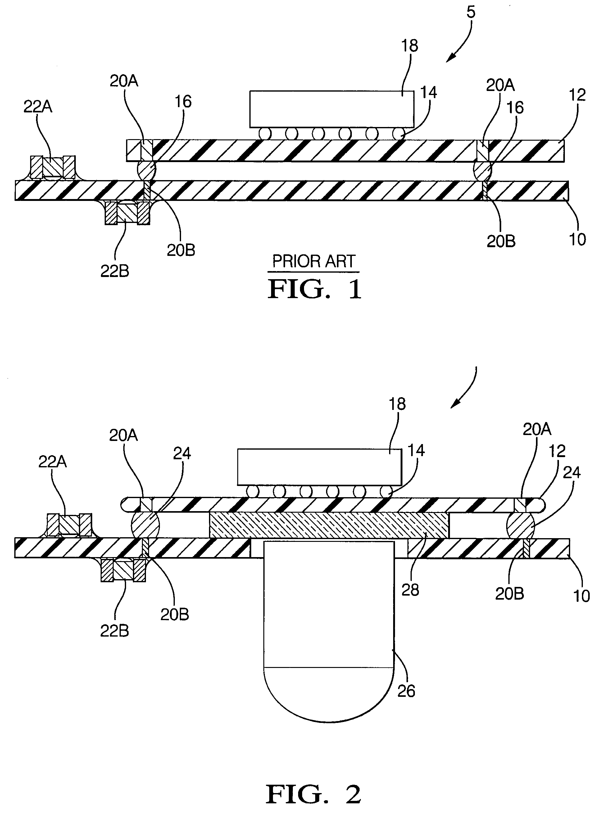
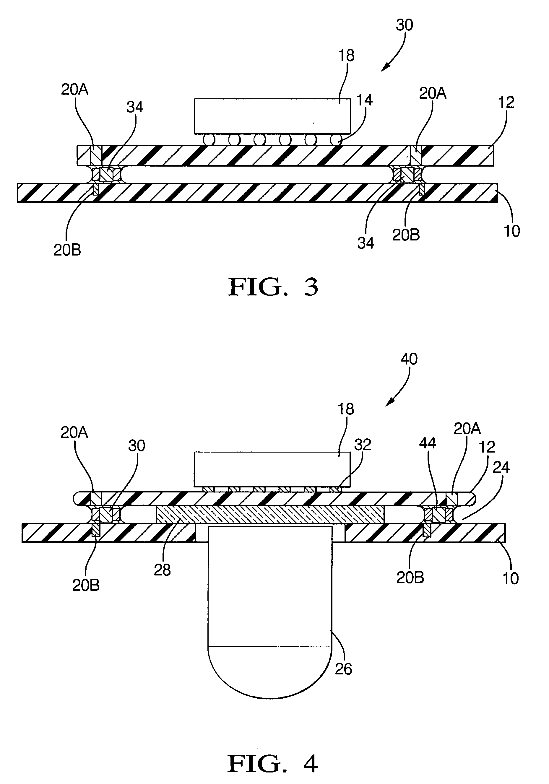
[0020]Exemplary embodiments are described with reference to specific configurations. Those of ordinary skill in the art will appreciate that various changes and modifications can be made while remaining within the scope of the appended claims. Additionally, well-known elements, devices, components, methods, process steps and the like may not be set forth in detail in order to avoid obscuring the invention. Further, unless indicated to the contrary, any numerical values set forth in the following specification and claims are approximations that may vary depending upon the desired characteristics sought to be obtained by the present invention.

[0021]An apparatus and method is described herein for attaching a first substrate to a second substrate for an electrical circuit assembly. The applicable forms of substrates include a printed circuit board such as a motherboard and a daughterboard. The present invention can further attach a semiconductor device to a substrate, the applicable for...


PUM


Abstract

A passive surface mount part such as a capacitor or a resistor is employed to attach a first substrate to a second substrate, or a semiconductor device to a substrate, for an electrical circuit assembly. Applicable forms of substrates include a printed circuit board such as a motherboard and a daughterboard, and applicable forms of semiconductor devices include an integrated circuit. In an aspect, a low profile attachment is provided forming a planar structure. Space is conserved, signal transmission is provided, and electrical performance is increased. In another aspect, a standoff is defined between the substrates setting the substrates apart a desired distance, compensating for any surface irregularities, increasing thermal separation, and increasing interconnect flexibility. As an application, the standoff defined between the substrates can be utilized for a structure such as optical glass structure to be situated between the substrates for use with an optical circuit assembly.

Description

FIELD OF THE INVENTION[0001]The invention relates generally to an interconnect for an electrical circuit substrate, and more particularly to utilizing a passive surface mount part such as a capacitor or resistor as an interconnect between a motherboard and a daughterboard or between an integrated circuit and a printed circuit board.BACKGROUND OF THE INVENTION[0002]Surface-mount technology is used to construct electronic circuits in which the components are mounted directly onto the surface of a printed circuit board (PCB). An electronic device so made is called a surface-mount device (SMD). In industry, SMDs have largely replaced through-hole technology, a previous construction method of fitting components with wire leads into holes in the PCB.[0003]A ball grid array (BGA) is a type of surface-mount packaging used for integrated circuits. Previously, a pin grid array (PGA) was used, which is a package with one face at least partly covered with pins in a grid pattern. These pins are ...

Claims


Application Information

Patent Timeline
IPC IPC(8): H05K7/02
CPCH05K1/023H05K1/0274H05K1/141H05K1/145H05K3/303H05K3/3436H05K2201/2036H05K2201/09072H05K2201/10121H05K2201/10636H05K2201/10727H05K2201/10734H05K3/368Y02P70/50
Inventor BURNS, JEFFREY H.DELHEIMER, CHARLES I.
Owner DELPHI TECH INC
Why Eureka
Try Eureka