Micron gap thermal photovoltaic device and method of making the same

a thermal photovoltaic and micro-gap technology, applied in the manufacture of cables/conductors, pv power plants, coatings, etc., can solve the problems of uncontrollable power output variance, temperature increase, and inability to effectively collect electrons, etc., to achieve the effect of convenient manufacturing

Active Publication Date: 2008-09-18
CHARLES STARK DRAPER LABORATORY
View PDF12 Cites 12 Cited by
  • Summary
  • Abstract
  • Description
  • Claims
  • Application Information

AI Technical Summary

Benefits of technology

[0013]It is therefore an object of this invention to provide a novel micron gap thermal photovoltaic device structure which is also easier to manufacture.
[0014]It is a further object of this invention to provide such a micron gap thermal photovoltaic device which results in high thermal isolation between the emitter and the photovoltaic substrate.
[0015]It is a further object of this invention to provide such a micron gap thermal photovoltaic device which can have a large area and is capable of high yield.
[0017]It is a further object of this invention to provide such a micron gap thermal photovoltaic device which is efficient.
[0019]It is a further object of this invention to provide such a micron gap thermal photovoltaic device which provides greater energy transfer.
[0023]This invention results from the realization a) that more uniform sub-micron gap thermal photovoltaic device which is easier to manufacture is effected by the use of a sacrificial layer between the emitters and their associated standoffs located right on the photovoltaic substrate and wherein the sacrificial layer is removed by chemical etching techniques to form the sub-micron gap between the lower planar surfaces of the emitters and the photovoltaic substrate thus eliminating the problems associated with multi-piece construction methods of the prior art; and b) that individual panels on one side (hot or cold) optionally connected by laterally compliant members, allows permanent connection of the center of these panels to the opposite side consistent with the sacrificial approach.

Problems solved by technology

While it is possible to obtain the sub-micron gap spacing, the thermal effects on the hot and cold surfaces induce cupping, warping, or deformation of the elements resulting in variations in gap spacing thereby resulting in uncontrollable variances in the power output.
Temperature increases, however, are limited by the material of the device and system components.
At high temperatures, intrinsic carrier generation swamps the PN junction and it is no longer an effective collector of electrons.
The micron gap thermal photovoltaic devices constructed to date according to the disclosure of the '546 patent have typically been small chips four square millimeters in area and not particularly well suited for the generation of sufficient electrical power in some applications.
This manufacturing technique could be difficult to accomplish on large area devices with dimensions on the order of inches or even feet.

Method used


Image

  • Micron gap thermal photovoltaic device and method of making the same
  • Micron gap thermal photovoltaic device and method of making the same
  • Micron gap thermal photovoltaic device and method of making the same

Examples


Embodiment Construction

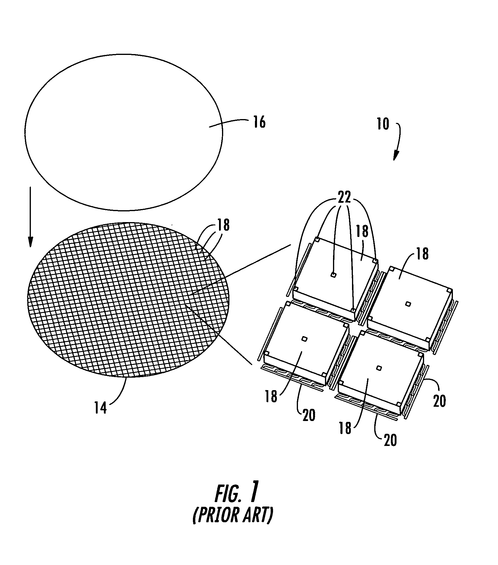
[0060]Thermal photovoltaic generator 10, FIG. 1, as disclosed in U.S. Pat. No. 6,232,546, includes emitters 18 on panel 14 supported thereon by flexors 20. The top surface of the emitters are spaced from photovoltaic device 16 by spacers 22 formed on each emitter. As such, photovoltaic device 16 and panel 14 must be joined together. Given that the gap between the top surface of each emitter and photovoltaic device 16 is typically less then one micron, particles can contaminate the resulting structure and topological surface variations and other surface defects can pose manufacturing difficulties. Moreover, the high temperatures associated with the emitters can cause deformation or breakage of the emitter / flexure / panel structures.

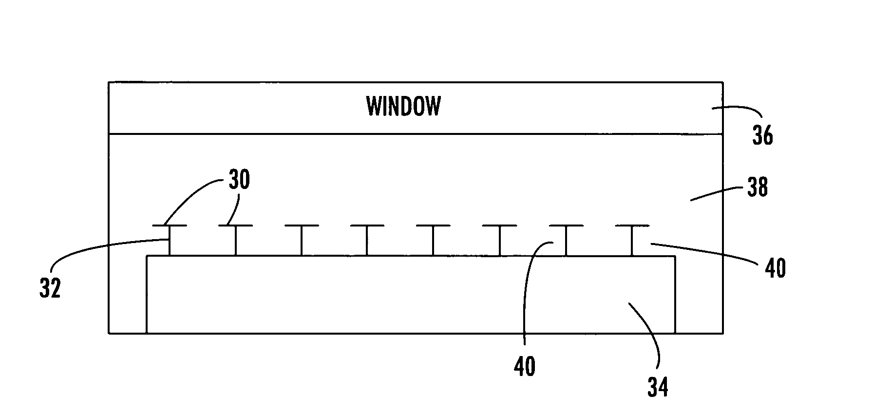
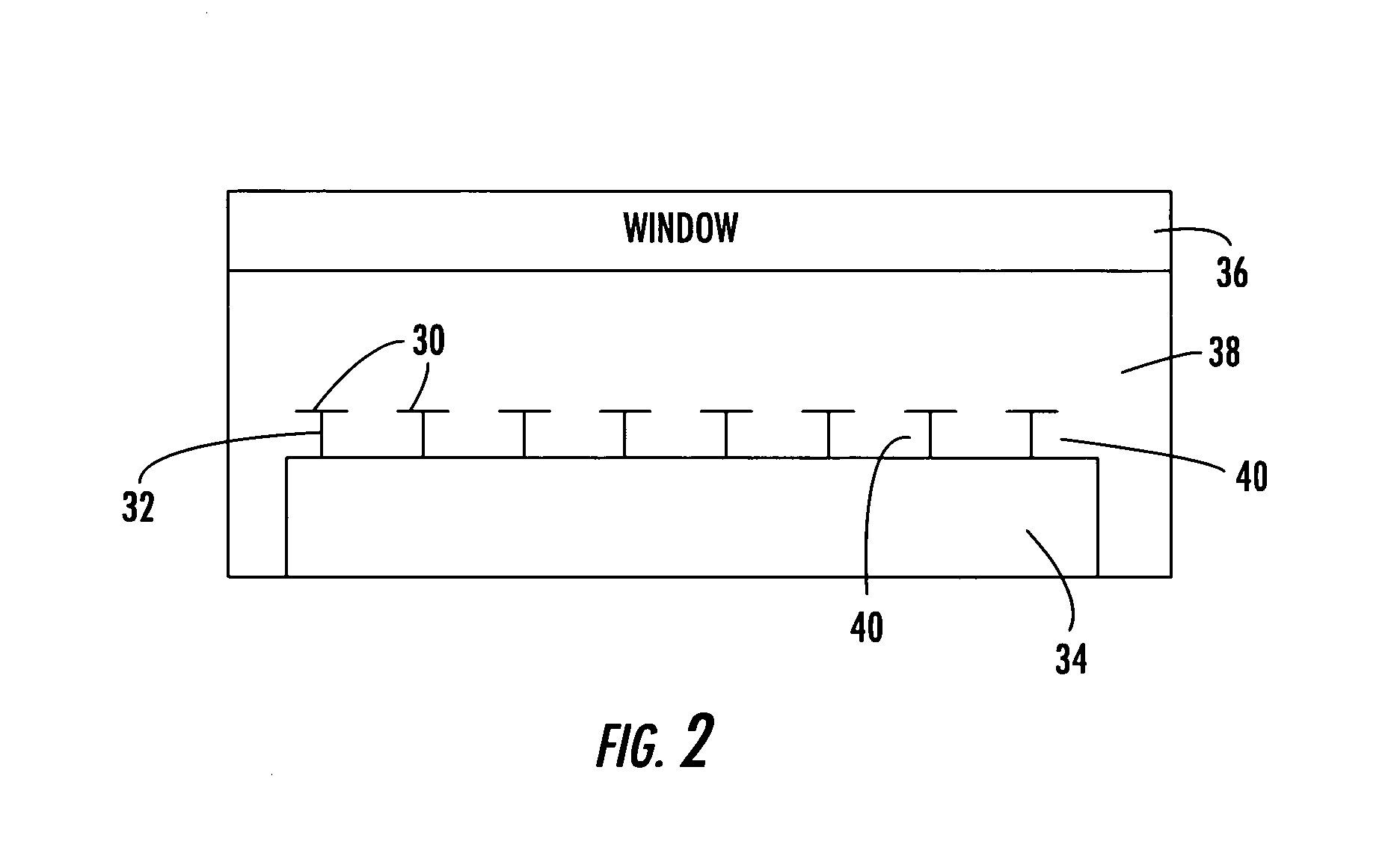
[0061]In the invention described herein, the emitters 30, FIG. 2 and their standoffs 32 upstanding from photovoltaic substrate 34 are formed directly on photovoltaic substrate 34 using deposition, patterning, and etching techniques thus eliminating the need ...


PUM

PropertyMeasurementUnit
thicknessaaaaaaaaaa
heightaaaaaaaaaa
heightaaaaaaaaaa

Abstract

A method of making a micron gap thermal photovoltaic device wherein at least one standoff is formed on a photovoltaic substrate, a sacrificial layer is deposited on the photovoltaic substrate and about the standoff, an emitter is attached to the standoff and has a lower planar surface separated from the photovoltaic substrate by the sacrificial layer, and the sacrificial layer is removed to form a sub-micron gap between the photovoltaic substrate and the lower planar surface of the emitter.

Description

RELATED APPLICATIONS[0001]This application is a divisional application of prior U.S. patent application Ser. No. 10 / 443,414 filed May 22, 2003 which is incorporated herein by reference.FIELD OF THE INVENTION[0002]This invention relates to thermal photovoltaic devices and more particularly to a microscale thermophotovoltaic generator.BACKGROUND OF THE INVENTION[0003]It has been shown that electromagnetic energy transfer between a hot and cold body is a function of the close spacing of the bodies due to evanescent coupling of near fields. Thus, the closer the bodies, approximately one micron and below, the greater the power transfer. For gap spacings of 0.1 microns, increases in the rate of energy transfer of factors of five and higher are observed.[0004]The dilemma, however, is forming and then maintaining the close spacing between two bodies at a sub-micron gap in order to maintain enhanced performance. While it is possible to obtain the sub-micron gap spacing, the thermal effects o...

Claims


Application Information

Patent Timeline
Patent Type & Authority Applications(United States)
IPC IPC(8): H01L31/04H01L31/18H01B13/00H01L31/00
CPCH02S10/30Y02E10/50
Inventor GREIFF, PAULDIMATTEO, ROBERT STEPHEN
Owner CHARLES STARK DRAPER LABORATORY
Why Eureka
Try Eureka