Semiconductor Structure of Liquid Crystal Display and Manufacturing Method Thereof

a liquid crystal display and semiconductor technology, applied in semiconductor/solid-state device manufacturing, semiconductor devices, electrical devices, etc., can solve the problems of more photo masks, more production time, and high production costs, so as to reduce the number of photo masks, increase production rate, and reduce production costs

Active Publication Date: 2008-09-18
AU OPTRONICS CORP
View PDF5 Cites 15 Cited by
  • Summary
  • Abstract
  • Description
  • Claims
  • Application Information

AI Technical Summary

Benefits of technology

[0009]In view of the foregoing, it is an objective of the invention to decrease the number of photo masks required in the manufacturing process, thereby reducing the production cost and increasing the production rate.

Problems solved by technology

However, it is well-known that photo masks are expensive.
More photo masks cost more.
Beside, the production time takes more.

Method used


Image

  • Semiconductor Structure of Liquid Crystal Display and Manufacturing Method Thereof
  • Semiconductor Structure of Liquid Crystal Display and Manufacturing Method Thereof
  • Semiconductor Structure of Liquid Crystal Display and Manufacturing Method Thereof

Examples


Embodiment Construction

[0020]According to the invention, the excessive part of the metal layer for forming the via plugs can be removed at the same time when the photoresist layer is chemically stripped. This method does not only decrease the required number of photo masks, but also uses the via plugs to connect the drain and source of the TFT and the storage capacitor and the data line. The transparent electrode can connect with the above-mentioned devices through the via plugs, greatly improve the electrical connection quality between the transparent conductive layer and the devices. The present invention will be apparent from the following detailed description, which proceeds with reference to the accompanying drawings, wherein the same references relate to the same elements.

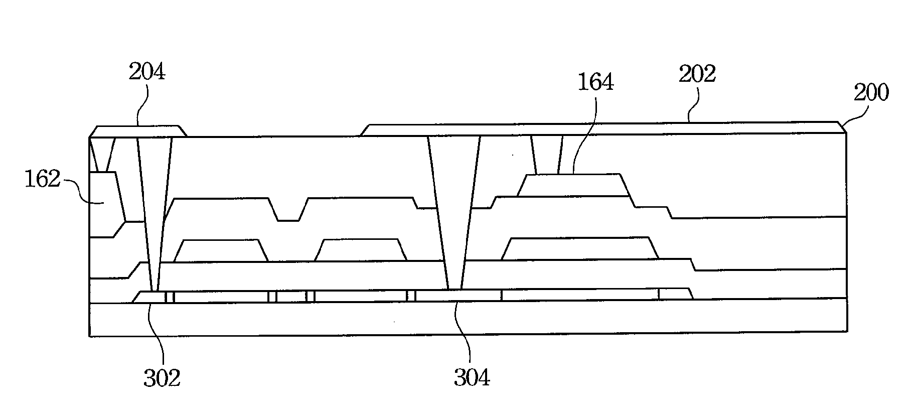
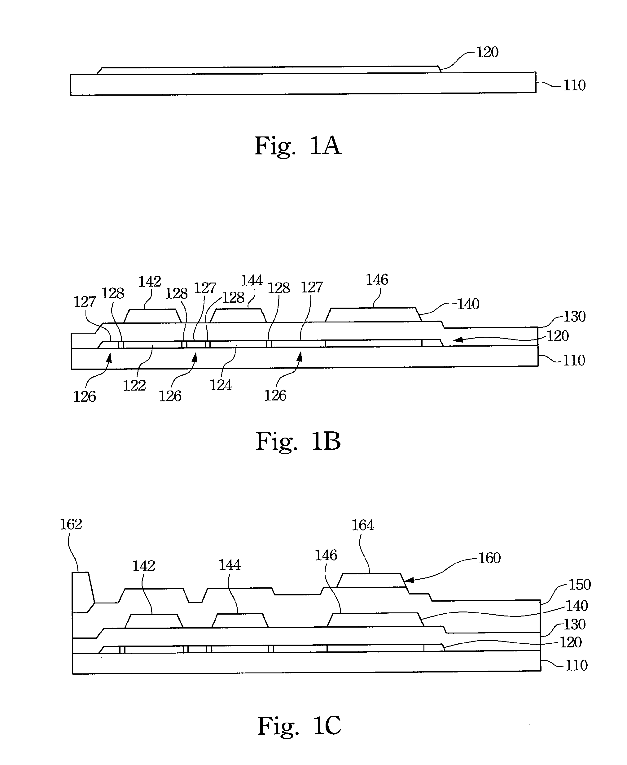
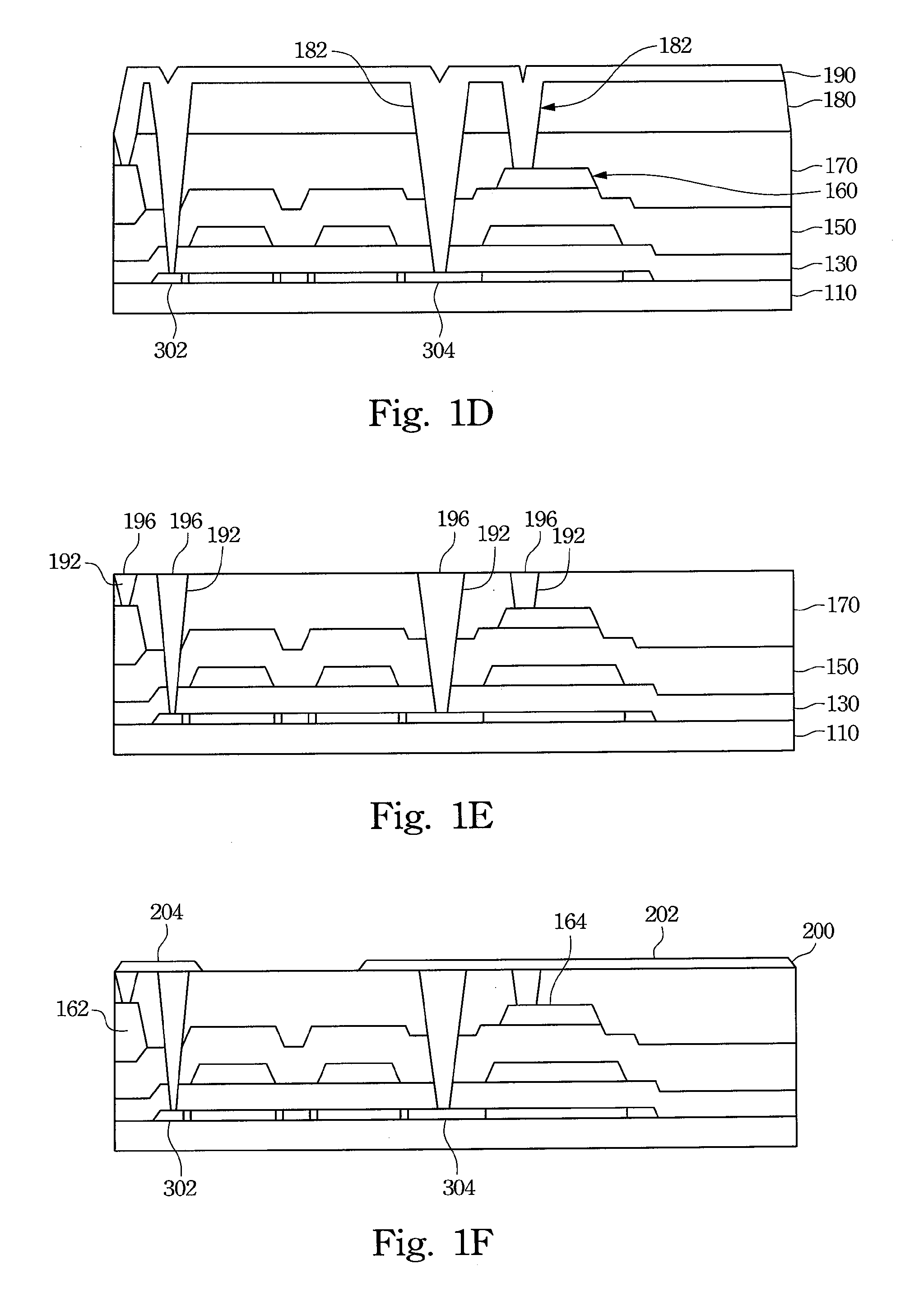
[0021]FIGS. 1A to 1F are schematic views showing steps in the disclosed method of manufacturing a semiconductor structure of an LCD panel. According to this embodiment, a substrate 110, such as a glass substrate or a quartz substra...


PUM


Abstract

A semiconductor structure of a liquid crystal display and the manufacturing method thereof are described. The manufacturing method includes the following steps. A patterned polysilicon layer and a first dielectric layer are formed on a substrate. A first patterned metal layer is formed to construct a gate electrode and a capacitor electrode. An ion implantation is conducted on the polysilicon layer to form drain and source electrodes. A second dielectric layer and a second patterned metal layer are formed thereon. Sequentially, a third dielectric layer is formed thereon. A plurality of via openings are formed by a patterned photoresist layer, and a third metal layer is formed thereon and filled into the via openings. The patterned photoresist layer and the redundant third metal layer are stripped from the substrate to form via plugs in the via openings. A patterned transparent conductive layer is formed thereon to connect the via plugs.

Description

RELATED APPLICATIONS[0001]This application claims priority to Taiwan Application Serial Number 96108833, filed Mar. 14, 2007, which is herein incorporated by reference.BACKGROUND OF THE INVENTION[0002]1. Field of Invention[0003]The invention relates to a semiconductor structure and, in particular, to a semiconductor structure of a liquid crystal display (LCD).[0004]2. Related Art[0005]In recent years, there has been a lot of progress in optoelectronic techniques. The coming digital era also pushes the rapid development in the LCD market. The LCD's have the advantages of high quality, small volume, light weight, low driving voltage, and low power consumption. Therefore, they are widely used in personal digital assistants (PDA), mobile phones, video cameras, laptop computers, desktop displays, vehicle displays, and projective televisions. They have gradually replaced the traditional cathode ray tubes (CRT) and become the main stream of displays.[0006]The LCD is a display device that u...

Claims


Application Information

Patent Timeline
Patent Type & Authority Applications(United States)
IPC IPC(8): H01L33/00H01L21/00
CPCH01L27/1288H01L27/1255
Inventor CHENG, YI-SHENGCHIU, TA-WEI
Owner AU OPTRONICS CORP
Why Eureka
Try Eureka