Method for forming fully silicided gate electrode in a semiconductor device

a technology of semiconductor devices and gate electrodes, which is applied in the direction of semiconductor devices, basic electric elements, electrical equipment, etc., can solve the problems of complex formation and integration of dual metal gates, adversely affecting device performance, and the size of semiconductor devices is increasing, so as to reduce the work function of semiconductor devices and reduce the equivalent oxide thickness (eot) of mos devices

Active Publication Date: 2008-09-18
UNITED MICROELECTRONICS CORP
View PDF5 Cites 16 Cited by
  • Summary
  • Abstract
  • Description
  • Claims
  • Application Information

AI Technical Summary

Benefits of technology

[0008]It is one object of the present invention to provide an improved fully silicided (FUSI) process to form fully silicided gate electrodes of a MOS device, which is capable of reducing work function thereof to reach NMOS band edge and also reducing the equivalent oxide thickness (EOT) of the MOS device.

Problems solved by technology

As semiconductor technology advances, semiconductor devices are becoming increasingly smaller.
However, this scaling down of devices may cause problems.
For example, as gate oxides are scaled down, gate capacitance due to polysilicon depletion issues becomes more problematic, adversely affecting device performance.
However, the formation and integration of these dual metal gates are complex tasks as compared to form traditional doped polysilicon gates.
However, it is still an issue to achieve real band-edge work function modulation.

Method used


Image

  • Method for forming fully silicided gate electrode in a semiconductor device
  • Method for forming fully silicided gate electrode in a semiconductor device
  • Method for forming fully silicided gate electrode in a semiconductor device

Examples


Embodiment Construction

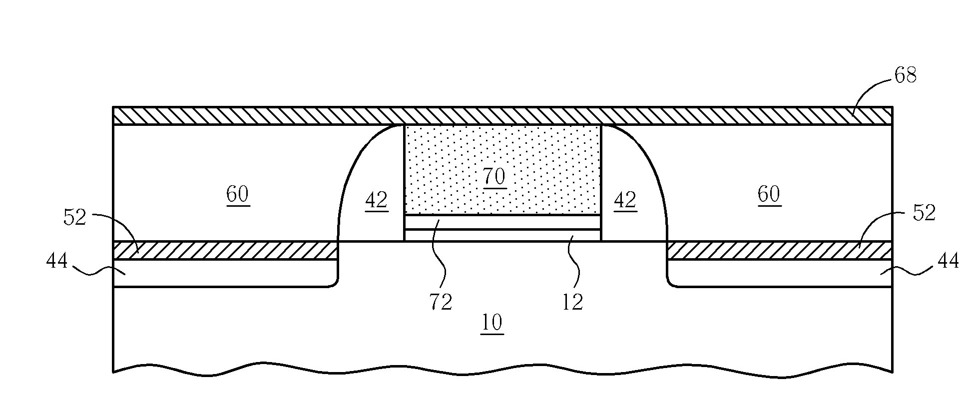
[0023]According to one aspect of the present invention, it is proposed to incorporate ytterbium (Yb) implantation (or implantation of other suitable elements) into nickel fully silicided (Ni-FUSI) process in order to reduce NMOS work function such that the work function can reach so-called NMOS band edge.

[0024]It is advantageous to use the present invention method because Yb implantation also effectively reduces the equivalent oxide thickness (EOT) of the silicon oxy-nitride (SiON) gate dielectric.

[0025]While it has been established, that the vacuum work function can not be realized in a metal / dielectric system, Yb has shown a great potential to reduce the work function of a Ni FUSI gate electrode, which would otherwise be close to mid gap. However, the mechanism of work function reduction by Yb is still not yet clear. It is believed that the work function shift may be caused by Yb pile-up at the interface of NiSi / dielectric during the NiSi formation.

[0026]It has been surprisingly f...


PUM


Abstract

A semiconductor MOS device includes a semiconductor substrate; a gate oxide layer disposed on the semiconductor substrate; a fully silicided gate electrode disposed on the gate oxide layer; a composite thin film interposed between the fully silicided gate electrode and the gate oxide layer; a spacer on sidewall of the fully silicided gate electrode; and a source/drain region implanted into the semiconductor substrate next to the spacer. A method for forming the semiconductor MOS device is disclosed.

Description

BACKGROUND OF THE INVENTION[0001]1. Field of the Invention[0002]The present invention relates generally to semiconductor processing. More specifically, the present invention relates to a method for forming fully silicided gate electrodes in a semiconductor device.[0003]2. Description of the Prior Art[0004]As semiconductor technology advances, semiconductor devices are becoming increasingly smaller. However, this scaling down of devices may cause problems. For example, as gate oxides are scaled down, gate capacitance due to polysilicon depletion issues becomes more problematic, adversely affecting device performance.[0005]One solution to this problem is the use of different metal gates for both NMOS and PMOS field effect transistors to serve as a replacement to polysilicon gates. However, the formation and integration of these dual metal gates are complex tasks as compared to form traditional doped polysilicon gates.[0006]Instead of the formation of dual metal gates, one type of tech...

Claims


Application Information

Patent Timeline
Patent Type & Authority Applications(United States)
IPC IPC(8): H01L21/336H01L29/78
CPCH01L21/28097H01L21/28229H01L29/78H01L29/513H01L29/518H01L29/4975
Inventor LIN, CHIEN-TINGCHENG, LI-WEIHSU, CHE-HUAHUANG, YAO-TSUNGMA, GUANG-HWA
Owner UNITED MICROELECTRONICS CORP
Why Eureka
Try Eureka