

Large area silicon cone arrays fabrication and cone based nanostructure modification
- Summary
- Abstract
- Description
- Claims
- Application Information
AI Technical Summary
Benefits of technology
Problems solved by technology
Method used
Image

Examples
example a
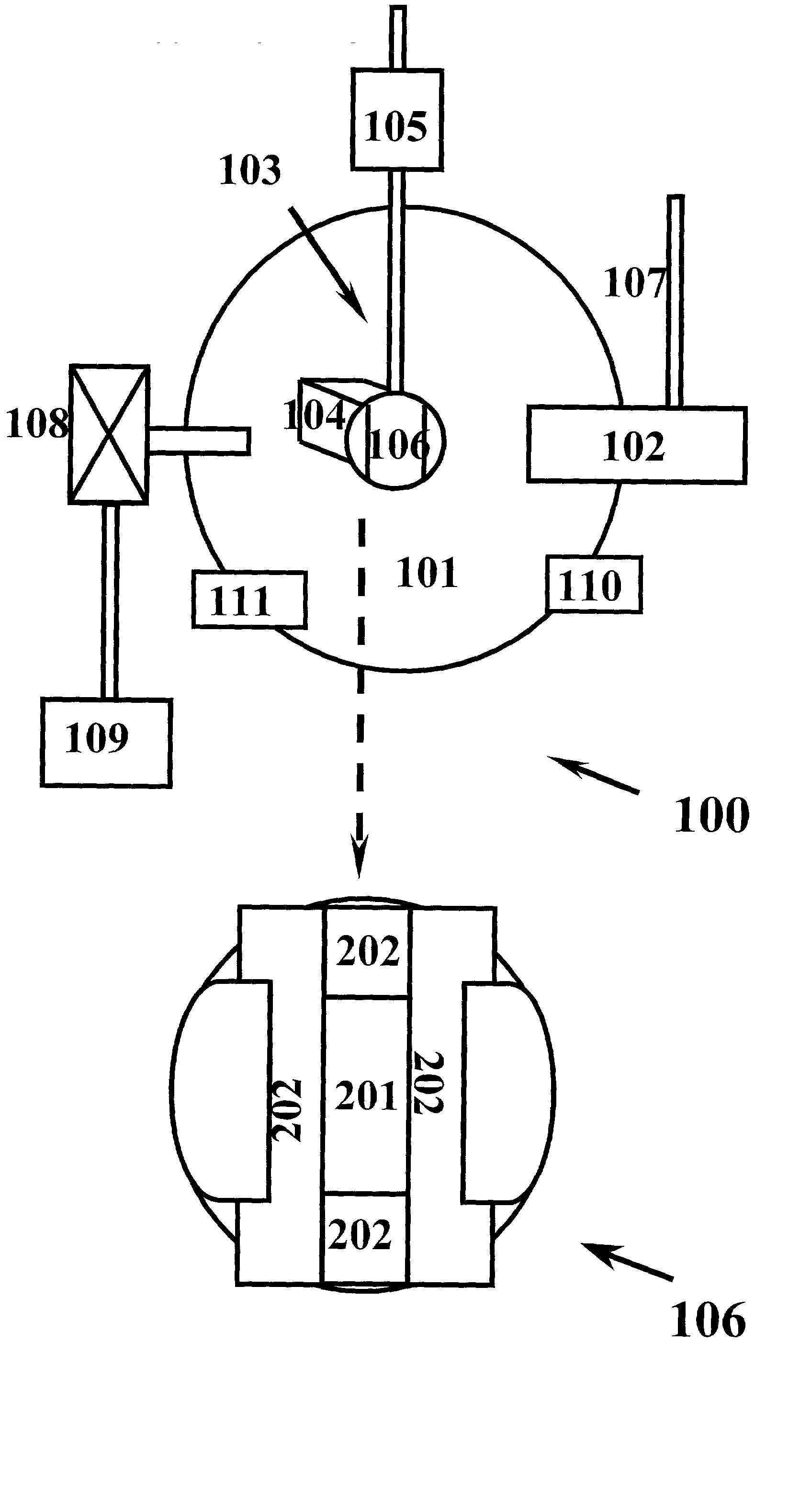
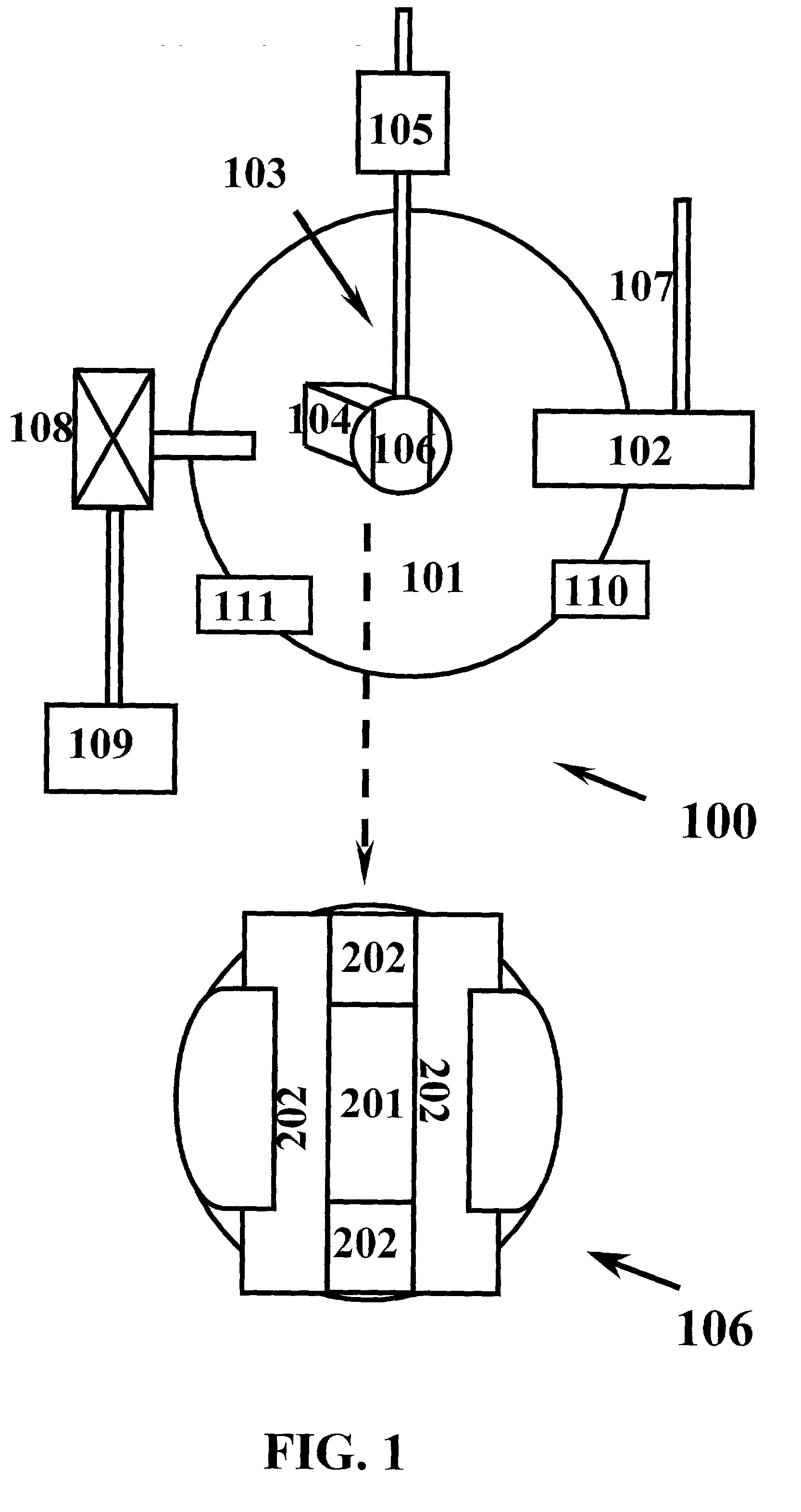
[0046] The silicon cone array for this sample was prepared in the apparatus shown in FIG. 1. Mirror polished silicon was used as the substrate. Nickel was used as the metal catalyst. The substrate temperature was maintained at 550.degree. C. Argon was used as the sputter gas and the total pressure was kept at 2.times.10.sup.-4 Torr. The ion energy was chosen at 900 eV and ion-current was 40 mA. The angle between the center ion-beam and the substrate surface normal is kept at 20 degree. The ion-sputtering time is 120 minutes.
[0047] Scanning Electron Microscopy (SEM) micrographs of the above sample are shown in FIG. 3. The 1 cm.times.2 cm silicon substrate is covered with uniform silicon cone arrays. The density of the cones is measured as 10.sup.8 / cm.sup.2. The height of each cone is up to several microns and the lateral size of the cone tip ranges from tens of nanometers to hundreds of nanometers. The contrast of the cone body and cone tip appears to be different, suggesting differe...
example b
[0048] The silicon cone array for this sample was prepared under the same experimental conditions as example A, except that tungsten was used as the metal catalyst.
[0049] SEM micrographs of the above sample are shown in FIG. 6. The 1 cm.times.2 cm silicon substrate is covered with uniform silicon cone arrays. The density of the cones is measured as 10.sup.8 / cm.sup.2. The height of each cone is up to several microns and the lateral size of the cone tip ranges from tens of nanometers to hundreds of nanometers. The contrast of the cone body and cone tip appears to be different, suggesting different chemical contents. EDX microanalysis shows that the cone body is composed of silicon and the cone tip is composed of silicon and tungsten (FIG. 7).
example c
[0050] The silicon cone array for this sample was prepared under the same experimental conditions as example A, except that molybdenum was used as the metal catalyst.
[0051] SEM micrographs of the above sample are shown in FIG. 8. The 1 cm.times.2 cm silicon substrate is covered with uniform silicon cone arrays. The density of the cones is measured as 10.sup.8 / cm.sup.2. The height of each cone is up to several microns and the lateral size of the cone tip ranges from tens of nanometers to hundreds of nanometers. The contrast of the cone body and cone tip appears to be different, suggesting different chemical contents. EDX microanalysis shows that the cone body is composed of silicon and the cone tip is composed of silicon and molybdenum (FIG. 9). Transmission electron microscopy (TEM) image shows different contrast of the cone body and cone tip (FIG. 10). Micro diffraction in FIG. 11 confirms that the cone body is single crystalline silicon (11a). The cone tip consists of several diff...
PUM
| Property | Measurement | Unit |
|---|---|---|
| Fraction | aaaaa | aaaaa |
| Fraction | aaaaa | aaaaa |
| Time | aaaaa | aaaaa |
Abstract
Description
Claims
Application Information