El display device and method for manufacturing same

Active Publication Date: 2014-06-12
JOLED INC
View PDF3 Cites 15 Cited by
  • Summary
  • Abstract
  • Description
  • Claims
  • Application Information

AI Technical Summary

Benefits of technology

[0013]In the EL display device relating to one aspect of the present invention, the common electrode is made of alkali metal or alkaline earth metal. Through the above configuration, formation of alkali metal oxide or alkaline earth metal oxide between the common electrode and the wiring, which conventionally occurs due to ITO, can be prevented. Therefore, the above configuration enables low contact resistance to be maintained between the

Problems solved by technology

As a consequence, an amount of electrical power supplied to the second electrode 1008 from the electrical supply wiring 1003 is decreased, which makes it difficult to effectively suppress the problem of voltage drop in the second electrode 1008.
Furthermore, the above prevents exciton-polaron quenching, and also prevents temporary reduction in internal quantum efficiency when power is switched on.
A main cause of the decre

Method used


Image

  • El display device and method for manufacturing same
  • El display device and method for manufacturing same
  • El display device and method for manufacturing same

Examples


embodiments

[0028]In one aspect of the present invention, an EL display device comprises: a substrate; a plurality of pixel electrodes located on the substrate with intervals therebetween; wiring located on the substrate in at least one of the intervals between the pixel electrodes; a plurality of light-emitting layer portions, each located on or above a corresponding one of the pixel electrodes in electrical connection therewith; a common electrode located on or above the light-emitting layer portions, and in electrical connection with the light emitting layer portions and the wiring; and a protective layer located on or above the common electrode, and preventing oxidization of the common electrode, wherein the common electrode is made of alkali metal or alkaline earth metal.

[0029]Alternatively, in another aspect of the present invention the EL display device may further comprise an intermediate layer including alkali metal or alkaline earth metal, located between the light-emitting layer port...

first embodiment

Overall Configuration of EL Display Device 1

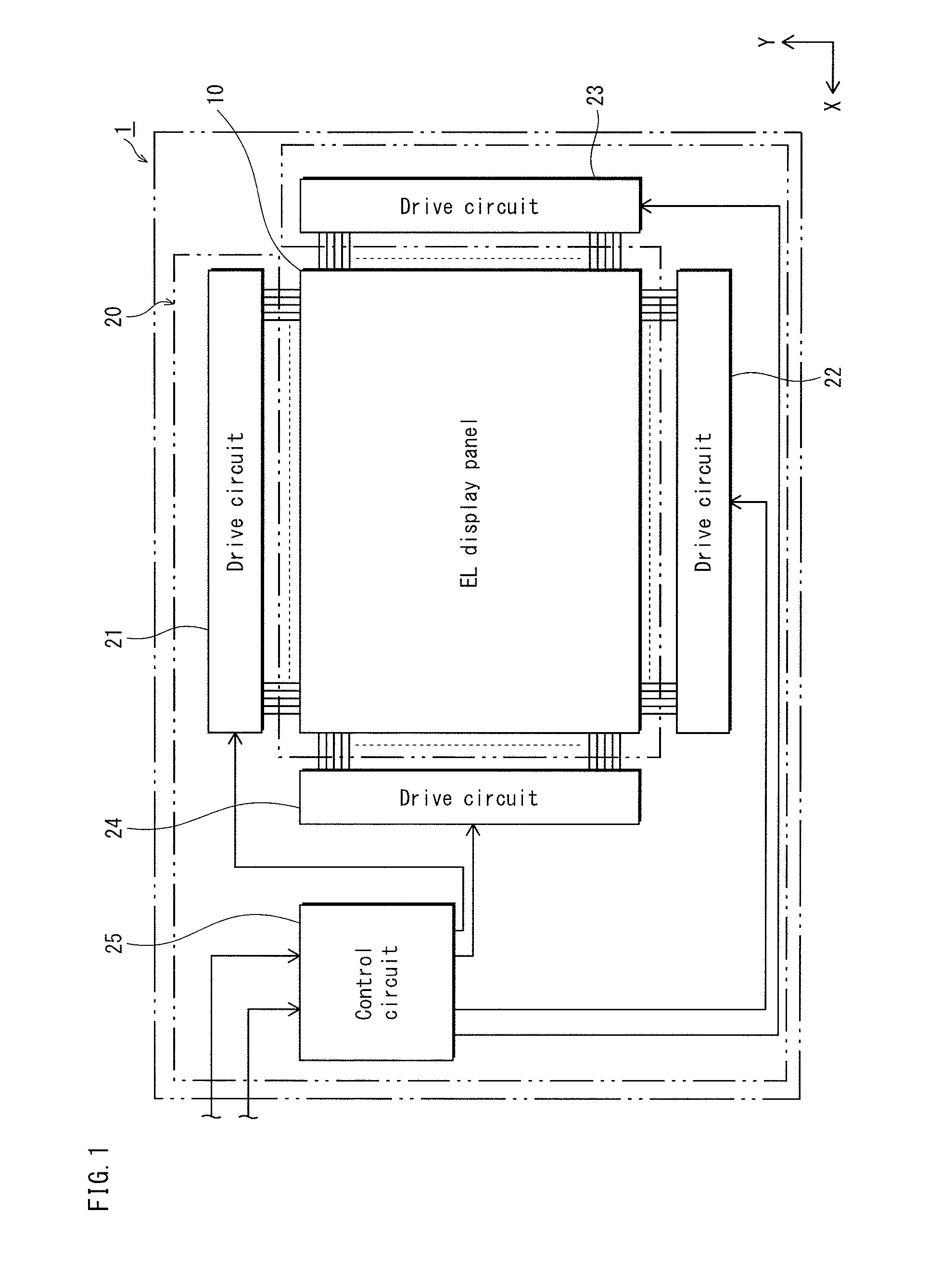
[0049]FIG. 1 is a block diagram that schematically illustrates overall configuration of an EL display device 1. The EL display device 1 includes an EL display panel 10 and a drive controller 20 which is connected to the EL display panel 10.

[0050]The EL display panel 10 is for example a top-emission organic EL display panel which uses electroluminescence of an organic material.

[0051]The drive controller 20 includes four drive circuits 21-24 and a control circuit 25.

[0052]In the EL display device 1, in terms of positioning of the drive controller 20 relative to the EL display panel 10, the drive controller 20 is not limited to being located surrounding four sides of the EL display panel 10 as illustrated in FIG. 1.

(Configuration of EL Display Panel 10)

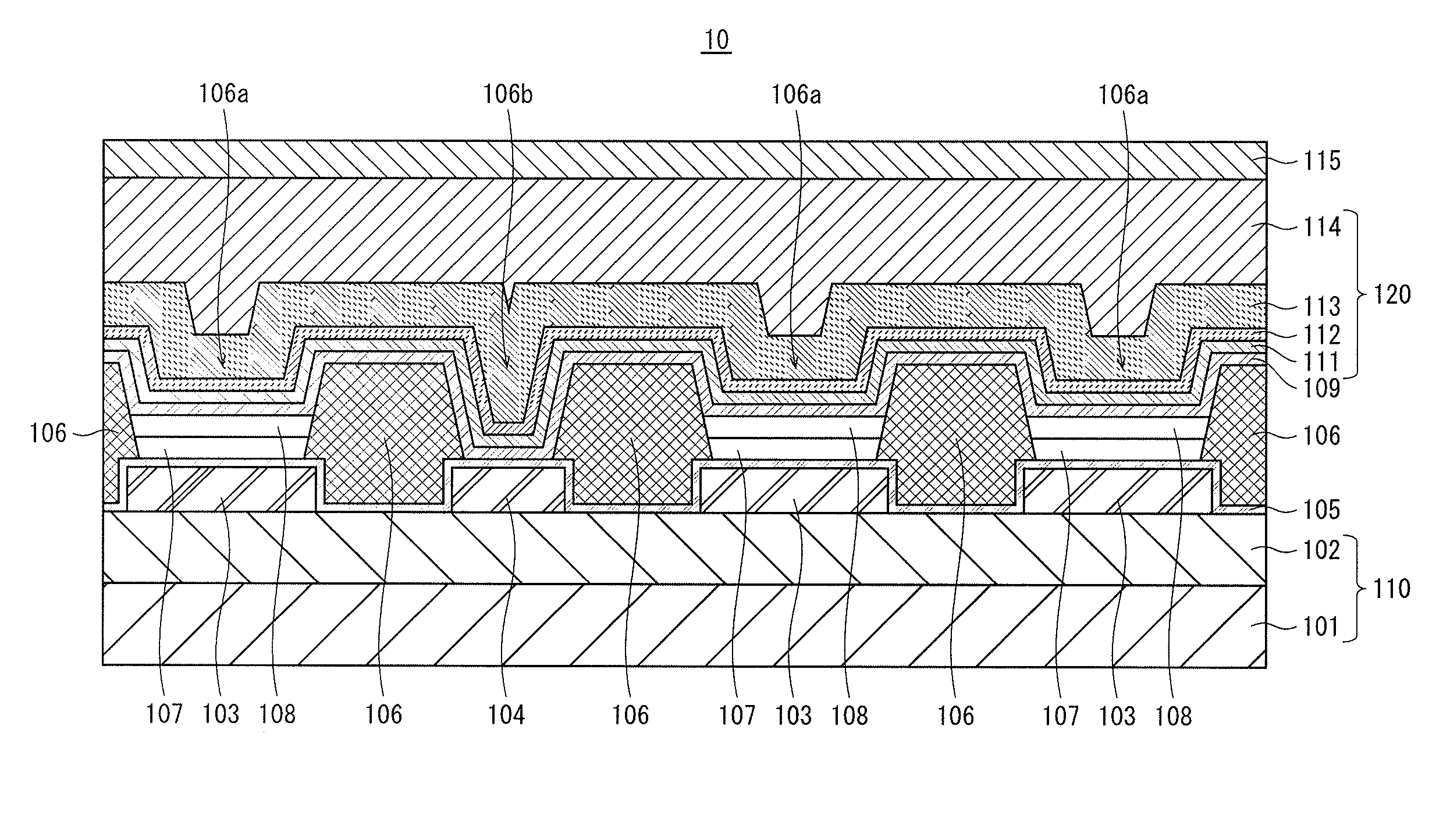
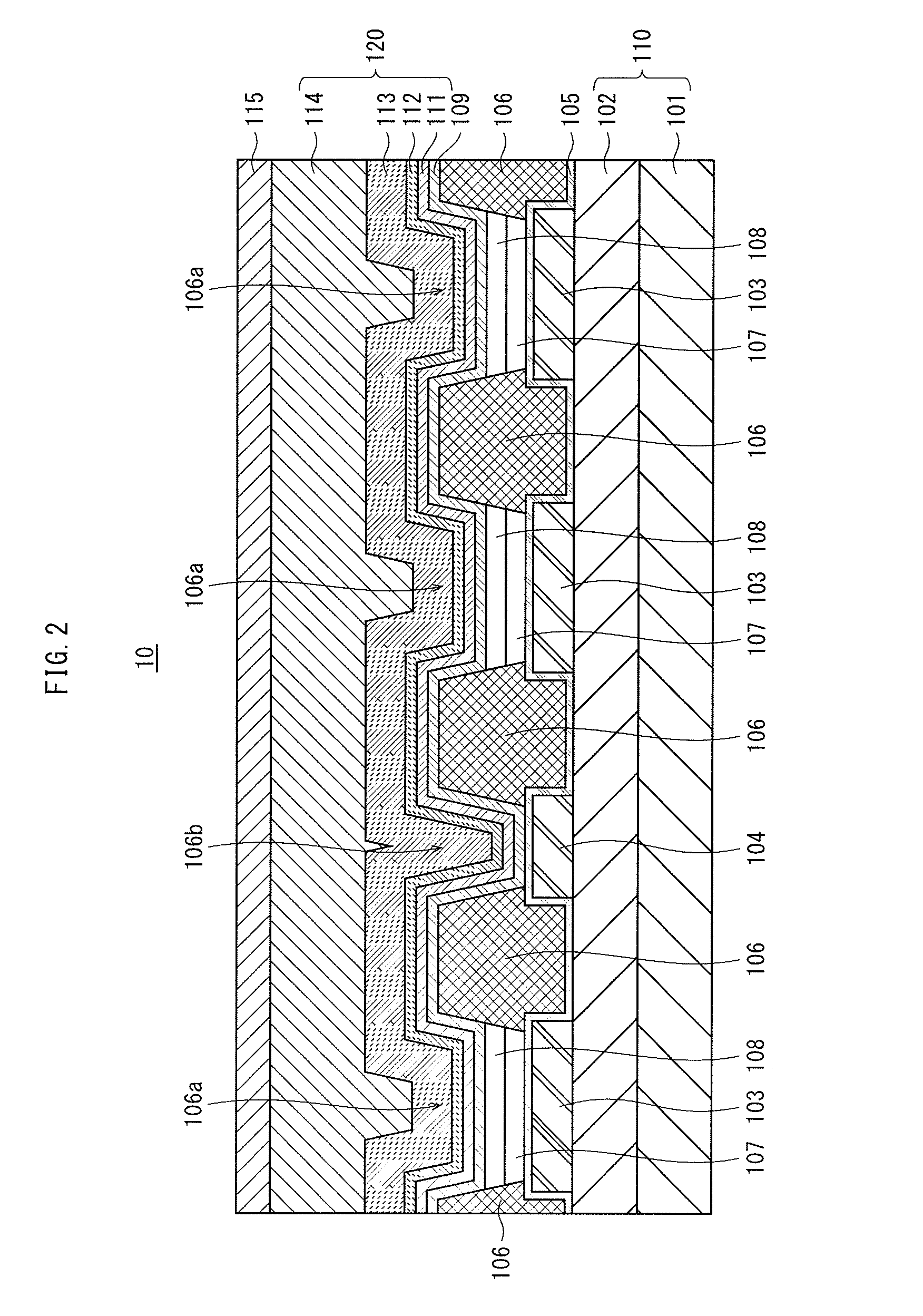
[0053]FIG. 2 is a partial cross-sectional diagram that schematically illustrates configuration of the EL display panel 10. FIG. 2 schematically illustrates one part of the EL display panel 10. ...

first modified example

[0112]The following explains a modified example in which an intermediate layer is located between a common electrode and a hole injection layer, above electrical supply wiring.

[0113]In the EL display panel 10 illustrated in FIG. 2, the electrical supply wiring 104 and the common electrode 109 are in electrical connection via the hole injection layer 105. Also, the common electrode 109 is made of alkali metal or alkaline earth metal. When the hole injection layer 105 is made of metal oxide including a transition metal oxide such as WOx, MoOx, or MoxWyOz, oxidization of the common electrode 109 may occur through the common electrode 109 stripping oxygen from the hole injection layer 105 due to a difference in electronegativity of the common electrode 109 and the hole injection layer 105. Through the above, the common electrode 109 is converted to an oxide insulator, and thus the problem of voltage drop may occur in the common electrode 109. One strategy for responding to the above pro...


PUM


Abstract

An EL display device of the present invention includes a plurality of pixel electrodes, wiring, a common electrode, a plurality of light-emitting layer portions, and a protective layer. The pixel electrodes are formed in one-to-one correspondence with a plurality of pixels. The wiring is formed in at least one of a plurality of intervals between the pixels. The common electrode is formed above each of the pixel electrodes and is in electrical connection with the wiring. The common electrode is made of alkali metal or alkaline earth metal. The light-emitting layer portions are each located between a corresponding one of the pixel electrodes and the common electrode. The protective layer is located on the common electrode, preventing oxidization thereof. The EL display device suppresses voltage drop in the common electrode, while also suppressing reduction in a property of electron injection to the light-emitting layer portions.

Description

TECHNICAL FIELD[0001]The present invention relates to an electroluminescence (EL) display device in which a light-emitting layer is located between a plurality of pixel electrodes, which are each located in a corresponding one of a plurality of pixels, and a common electrode which is common to all of the pixels. In particular, the present invention relates to an EL display device including wiring for supplying electrical power to the common electrode (referred to below as electrical supply wiring).BACKGROUND ART[0002]In a typical EL display device, a common electrode is located continuously throughout a plurality of pixels located on a substrate. An electrical voltage is applied to a portion of a light-emitting layer in each of the pixels, via the common electrode, from a periphery of the substrate. Consequently, due to electrical resistance of the common electrode, there is a tendency for electrical voltage applied to light-emitting layer portions in a central region of the substra...

Claims


Application Information

Patent Timeline
IPC IPC(8): H01L27/15H01L33/44H01L27/12
CPCH01L27/156H01L33/44H01L27/1262H05B33/26H10K59/179H10K50/828H10K50/844H10K59/122
Inventor ISOBE, TAKASHI
Owner JOLED INC
Why Eureka
Try Eureka