Low cost lead-free preplated leadframe having improved adhesion and solderability

a leadframe and low cost technology, applied in semiconductor devices, semiconductor/solid-state device details, thin material processing, etc., can solve the problems of difficult to maintain mold compound adhesion to leadframes, known leadframes do not offer metallization for good adhesion, etc., to achieve easy manufacturing, enhance down-bonding capability, and improve moisture-level quality

Active Publication Date: 2008-09-18
TEXAS INSTR INC
View PDF15 Cites 16 Cited by
  • Summary
  • Abstract
  • Description
  • Claims
  • Application Information

AI Technical Summary

Benefits of technology

[0010]A need has therefore arisen for a low cost, reliable leadframe combining adhesion to molding compounds, bondability for connecting wires, solderability of the exposed leadframe segments, and no risk of tin dendrite growth. There are technical advantages, when the leadframe and its method of fabrication is low cost and flexible enough to be applied for different semiconductor product families and a wide spectrum of design and assembly variations, and achieves improvements toward the goals of improved process yields and device reliability. There are further technical advantages, when these innovations are accomplished using the installed equipment base so that no investment in new manufacturing machines is needed.
[0012]In terms of preferred layer thicknesses, the nickel layer is between about 0.5 and 2.0 μm thick, the palladium layer between about 5 and 150 nm thick, and the tin layer less than about 5 nm thick, preferably about 3 nm. At this thinness, the tin has no capability of forming whiskers, but offers superb adhesion to polymeric encapsulation materials, improved characteristics for reliable stitch bonding as well as affinity to reflow metals (solders). By replacing the conventional gold layer, the tin layer offers a low cost alternative.
[0015]It belongs to the technical advantages of the invention that no toxic or whiskering materials are used for the plating steps, down-bonding capability is enhanced, and moisture-level quality is improved. Furthermore, the required plating processes are inexpensive and easy to manufacture.

Problems solved by technology

The recent general trend to avoid Pb in the electronics industry and use Pb-free solders, pushes the reflow temperature range into the neighborhood of about 260° C. This higher reflow temperature range makes it more difficult to maintain the mold compound adhesion to the leadframes.
For this temperature range, known leadframes do not offer metallization for good adhesion combined with low cost, easy manufacturability, and avoidance of whiskers.

Method used


Image

  • Low cost lead-free preplated leadframe having improved adhesion and solderability
  • Low cost lead-free preplated leadframe having improved adhesion and solderability

Examples


Embodiment Construction

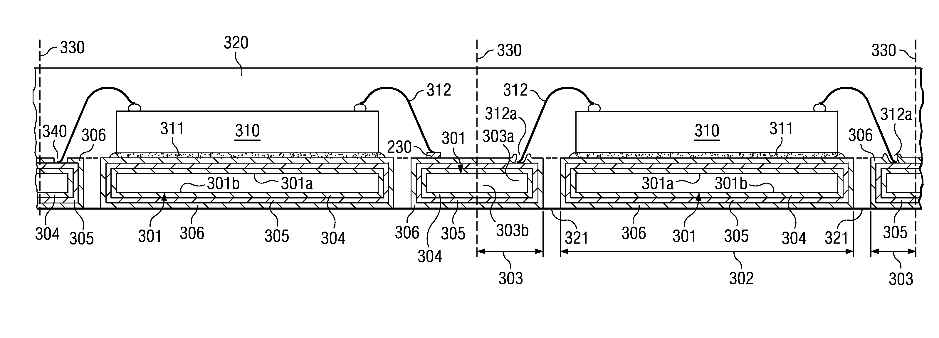
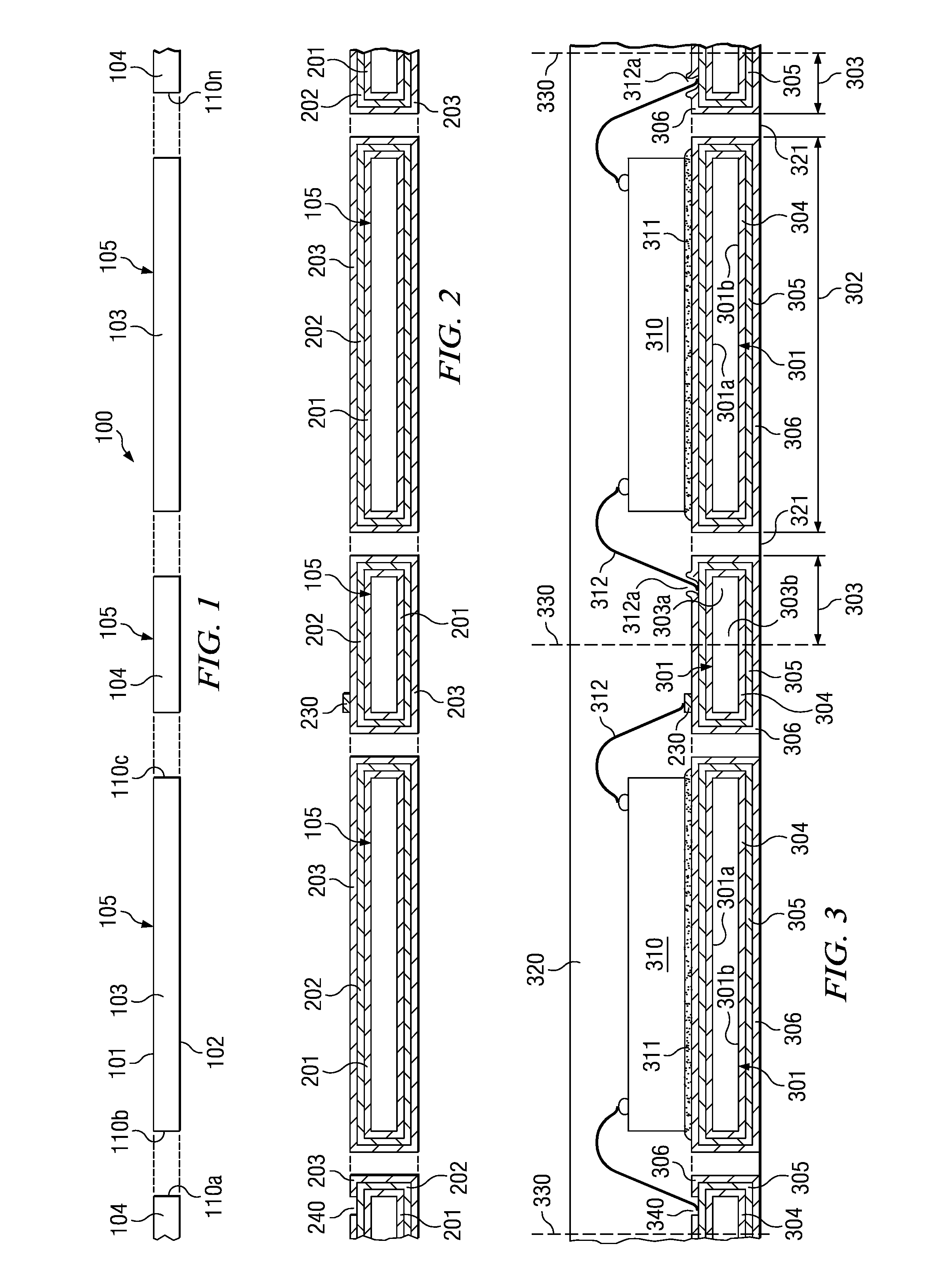
[0020]FIG. 1 is a schematic and simplified cross section of a leadframe portion, generally designated 100. The leadframe has a plurality of surfaces: the first surface 101, the second surface 102, and numerous side edge surfaces 110a, 110b . . . 110n. While the surfaces 101 and 102 originate from the sheet of starting material, the side edge surfaces 110a to 110n have been created by the forming process of the leadframe structure. The leadframe portion depicted contains a plurality of chip mount pads 103 and a plurality of lead segments 104. The leadframe is made of a base metal 105.

[0021]As defined herein, the starting material of the leadframe is called the “base metal”, indicating the type of metal. Consequently, the term “base metal” is not to be construed in an electrochemical sense (as in opposition to ‘noble metal’) or in a structural sense.

[0022]Base metal 105 is typically copper or a copper alloy. Other choices comprise brass, aluminum, iron-nickel alloys (“Alloy 42”), and ...


PUM

PropertyMeasurementUnit
thickaaaaaaaaaa
thickaaaaaaaaaa
temperatureaaaaaaaaaa

Abstract

A leadframe with a structure made of a base metal (105), wherein the structure has a plurality of surfaces. On each of these surfaces are metal layers in a stack adherent to the base metal. The stack comprises a nickel layer (201) in contact with the base metal, a palladium layer (202) in contact with the nickel layer, and an outermost tin layer (203) in contact with the palladium layer. In terms of preferred layer thicknesses, the nickel layer is between about 0.5 and 2.0 μm thick, the palladium layer between about 5 and 150 nm thick, and the tin layer less than about 5 nm thick, preferably about 3 nm. At this thinness, the tin has no capability of forming whiskers, but offers superb adhesion to polymeric encapsulation materials, improved characteristics for reliable stitch bonding as well as affinity to reflow metals (solders).

Description

[0001]This is a continuation of application Ser. No. 11 / 026,841 filed Dec. 30, 2004, the contents of which are herein incorporated by reference in its entiretyFIELD OF THE INVENTION[0002]The present invention is related in general to the field of semiconductor devices and processes, and more specifically to the materials and fabrication of leadframes for semiconductor devices.DESCRIPTION OF THE RELATED ART[0003]Leadframes for semiconductor devices provide a stable support pad for firmly positioning the semiconductor chip, usually an integrated circuit (IC) chip within a package. Since the leadframe, including the pad, is made of electrically conductive material, the pad may be biased, when needed, to any electrical potential required by the network involving the semiconductor device, especially the ground potential.[0004]In addition, the leadframe offers a plurality of conductive segments to bring various electrical conductors into close proximity of the chip. The remaining gap betw...

Claims


Application Information

Patent Timeline
Patent Type & Authority Applications(United States)
IPC IPC(8): H01L23/495H01L21/60
CPCH01L23/49582H01L24/48H01L24/97H01L2224/32245H01L2224/45144H01L2224/48091H01L2224/48247H01L2224/48465H01L2224/73265H01L2224/85464H01L2224/97H01L2924/01013H01L2924/01014H01L2924/01029H01L2924/01032H01L2924/01033H01L2924/01046H01L2924/01047H01L2924/0105H01L2924/01078H01L2924/01079H01L2924/01082H01L2924/01322H01L2924/10329H01L2924/14H01L24/45H01L2924/0132H01L2924/01006H01L2924/014H01L2924/01028Y10T428/1259H01L2924/00014H01L2224/83H01L2224/85H01L2924/00012H01L2924/00H01L24/73H01L2224/48664H01L2924/181
Inventor ABBOTT, DONALD C.
Owner TEXAS INSTR INC
Why Eureka
Try Eureka