Pixel circuit, display device, and driving method thereof

a technology of display device and pixel circuit, which is applied in the direction of static indicating device, electroluminescent light source, instruments, etc., can solve the problems of increasing voltage consumption, needing to increase the amplitude of video signal, and reducing light emission luminance, so as to prevent a decrease in light emission luminance, the driving potential during the emission period can be widened, and the effect of increasing the difference between the control input terminal and the output terminal of the drive transistor

Inactive Publication Date: 2008-09-18
SONY CORP
View PDF2 Cites 52 Cited by
  • Summary
  • Abstract
  • Description
  • Claims
  • Application Information

AI Technical Summary

Benefits of technology

[0025]According to an embodiment of the present invention, the capacitive element is added, and one terminal of the capacitive element is connected to the output terminal of the drive transistor and the other terminal of the capacitive element is supplied with the information corresponding to the pulse for starting the mobility correcting operation. Thereby the potential difference between the control input terminal and the output terminal of the drive transistor is increased.
[0026]When the sampling transistor is set in a conducting state to retain the information corresponding to the signal potential in the storage capacitor and then mobility correcting operation is performed while the sampling transistor is held in the conducting state, mobility correction can be made after

Problems solved by technology

Thus, because mobility correcting operation is performed in a state of the gate potential of the drive transistor being fixed, gate-to-source voltage is decreased due to mobility correction, which results in an adverse effect of a decrease in light emission luminance when no measure is taken against the decrease in

Method used


Image

  • Pixel circuit, display device, and driving method thereof
  • Pixel circuit, display device, and driving method thereof
  • Pixel circuit, display device, and driving method thereof

Examples


Embodiment Construction

[0039]Preferred embodiments of the present invention will hereinafter be described in detail with reference to the drawings.

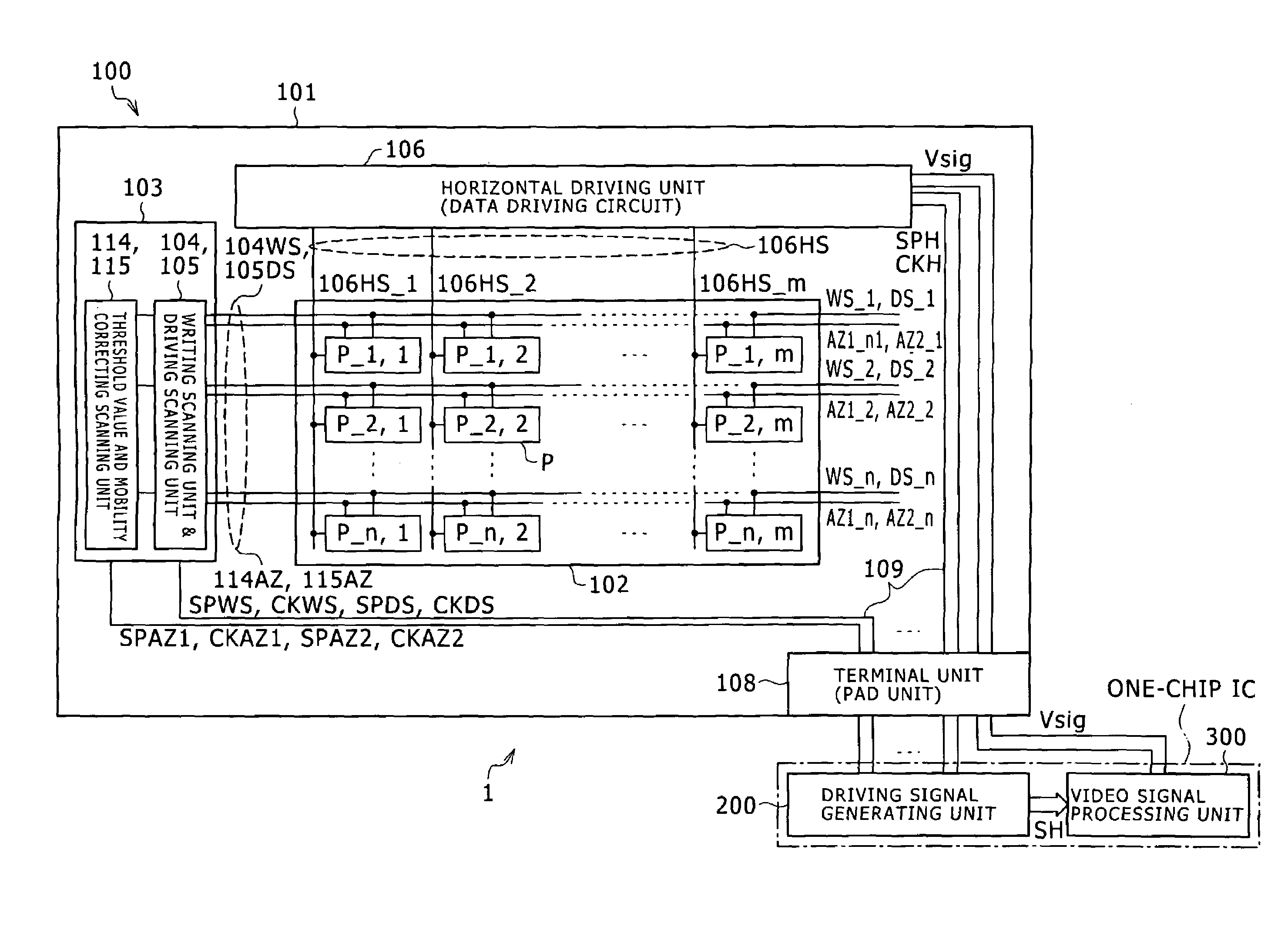
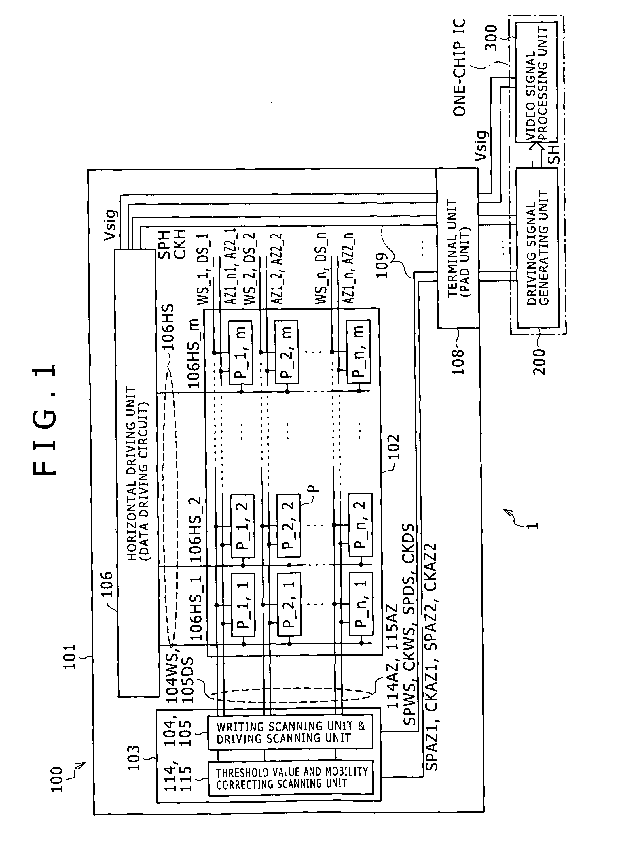
[0040]FIG. 1 is a block diagram schematically showing a configuration of an active matrix type display device as an embodiment of a display device according to the present invention. In the present embodiment, description will be made by taking as an example a case where the present invention is applied to an active matrix type organic EL display (hereinafter referred to as an organic EL display device) that for example uses an organic EL element as a display element of a pixel and a polysilicon thin film transistor (TFT) as an active element and which display is constituted with the organic EL element formed on a semiconductor substrate where the thin film transistor is formed.

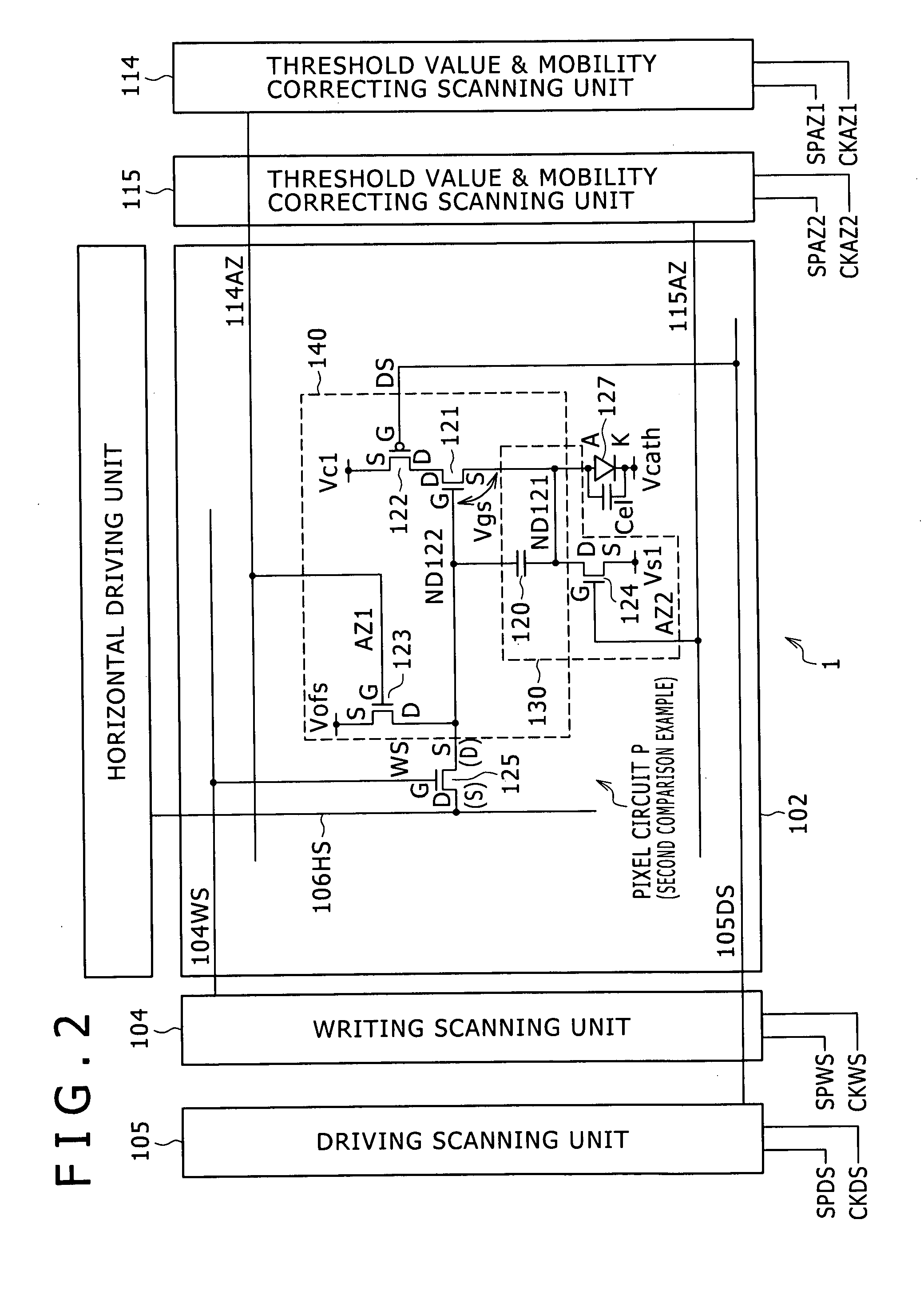
[0041]Incidentally, while concrete description will be made in the following by taking the organic EL element as the display element of the pixel as an example, the organic EL element is...


PUM


Abstract

Disclosed herein is a display device including a pixel array unit and a control unit.

Description

CROSS REFERENCES TO RELATED APPLICATIONS[0001]The present invention contains subject matter related to Japanese Patent Application JP 2007-068020 filed in the Japan Patent Office on Mar. 16, 2007, the entire contents of which being incorporated herein by reference.BACKGROUND OF THE INVENTION[0002]1. Field of the Invention[0003]The present invention relates to a pixel circuit (referred to also as a pixel) including an electro optic element (referred to also as a display element or a light emitting element), a display device having a pixel array unit in which such pixel circuits are arranged in the form of a matrix, and a driving method of the display device, and particularly to a pixel circuit having an electro optic element changing in luminance according to the magnitude of a driving signal as a display element, an active matrix type display device that is formed by arranging such pixel circuits in the form of a matrix and which device has an active element in each pixel circuit, d...

Claims


Application Information

Patent Timeline
IPC IPC(8): G06F3/038
CPCG09G3/3233G09G2300/0819G09G2320/043G09G2300/0861G09G2300/0842G09G3/20G09G3/30G09G3/32H05B33/12
Inventor TOYOMURA, NAOBUMIUCHINO, KATSUHIDEIIDA, YUKIHITO
Owner SONY CORP
Why Eureka
Try Eureka