Single poly EEPROM without separate control gate nor erase regions

a technology of eeprom and gate gate, which is applied in the field of modified otp eprom, can solve the problems of not being able to electrically erase without utilizing the expensive and inconvenient uv erase technology, and achieve the effect of reducing wafer manufacturing costs and siz

Active Publication Date: 2008-09-18
TEXAS INSTR INC
View PDF4 Cites 40 Cited by
  • Summary
  • Abstract
  • Description
  • Claims
  • Application Information

AI Technical Summary

Benefits of technology

[0016]Thus a simple and cost effective EEPROM memory device having a reduced size may be embedded with common CMOS devices to reduce wafer manufacturing costs.

Problems solved by technology

In addition, OTP EPROM is not electrically erasable without utilizing the expensive and very inconvenient UV erasure technologies.

Method used


Image

  • Single poly EEPROM without separate control gate nor erase regions
  • Single poly EEPROM without separate control gate nor erase regions
  • Single poly EEPROM without separate control gate nor erase regions

Examples


Embodiment Construction

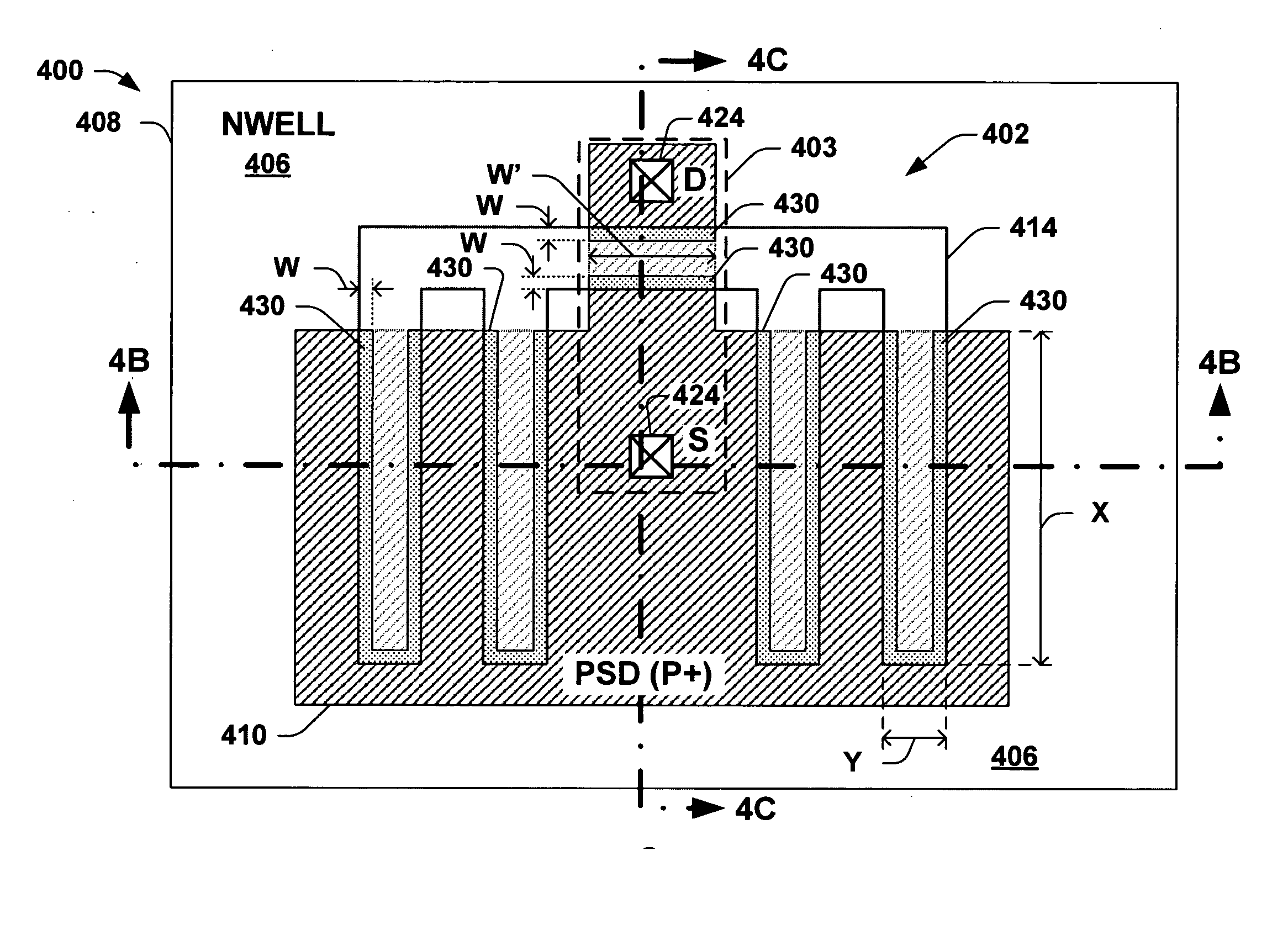
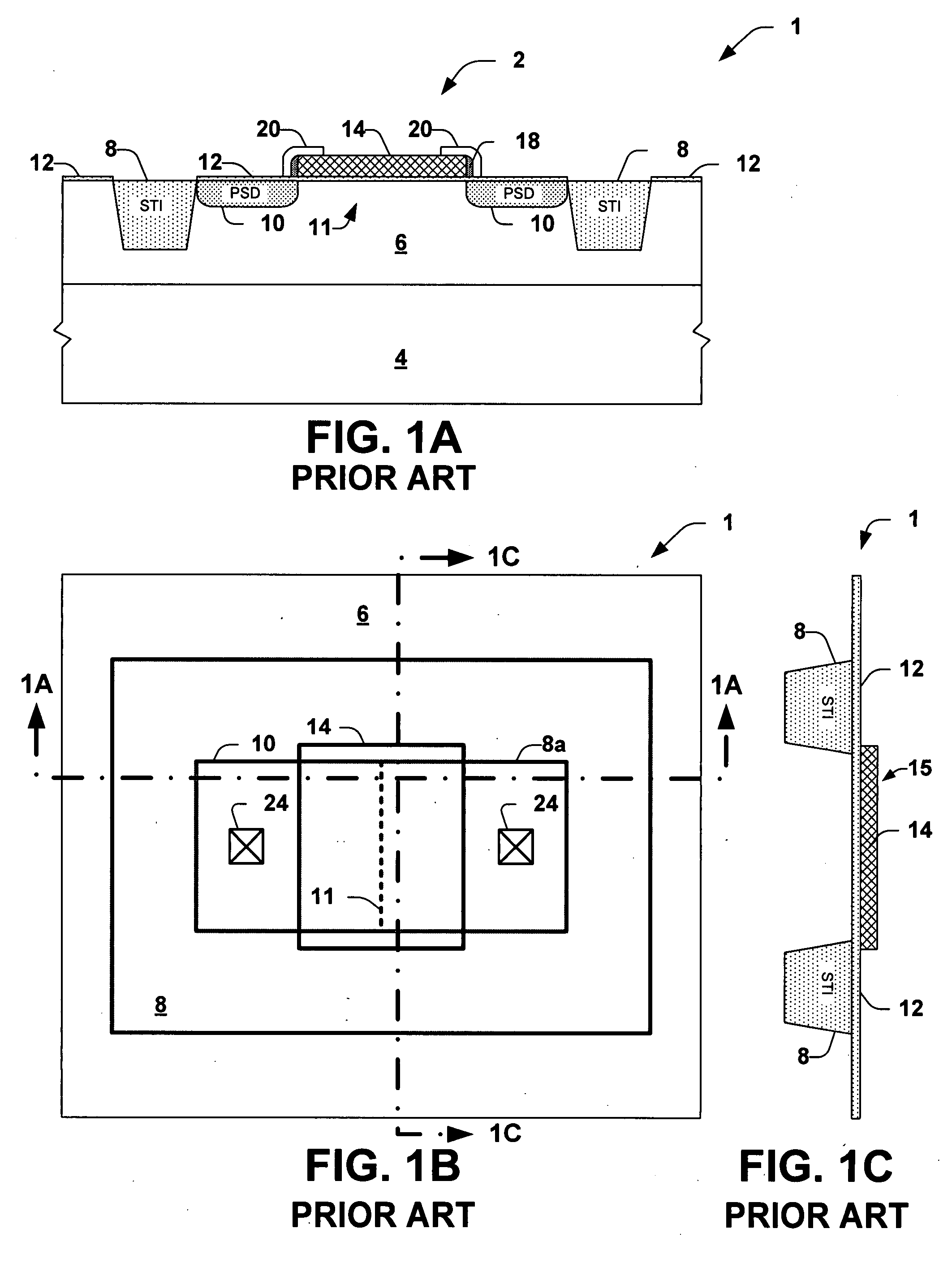
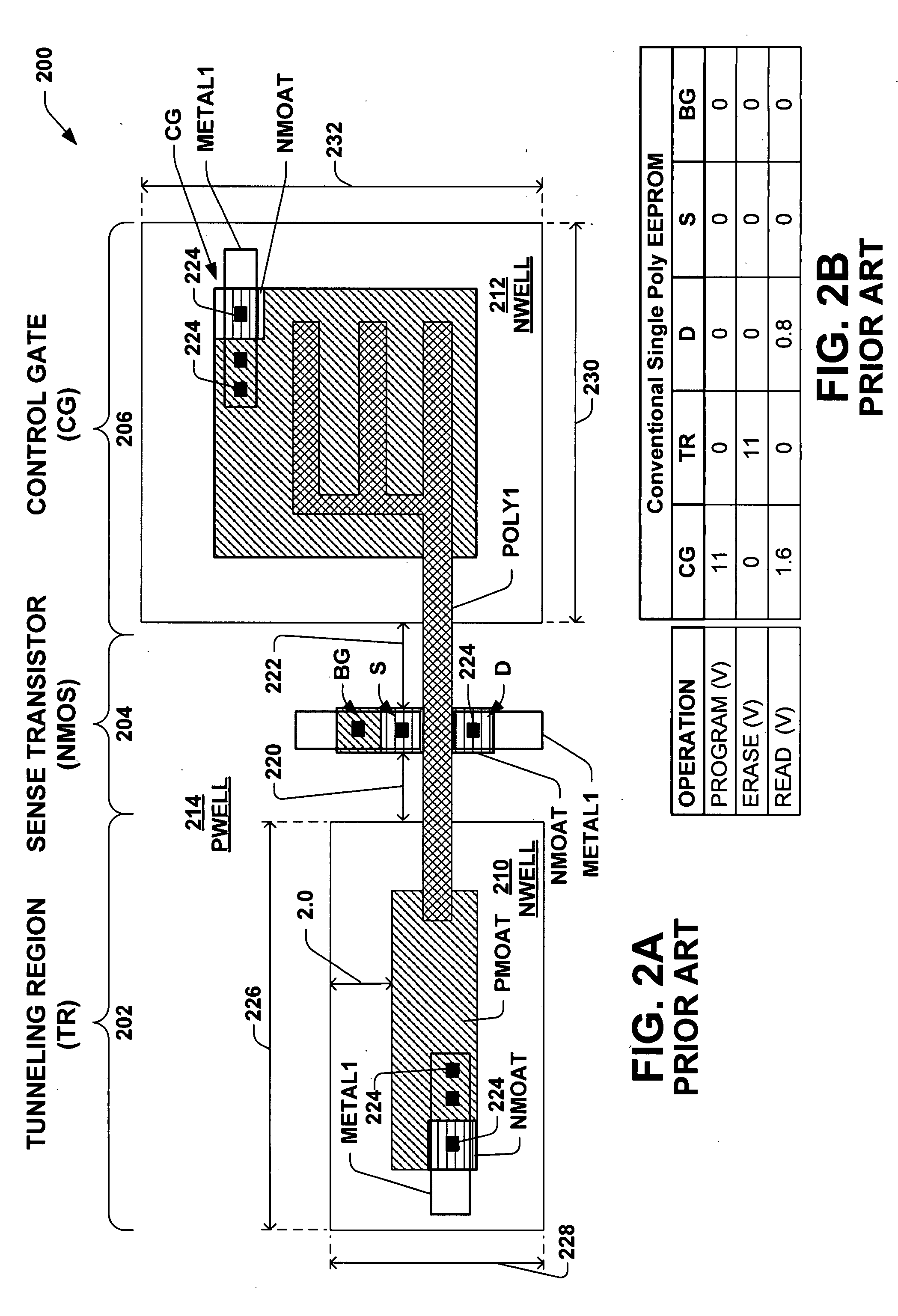
[0027]The present invention will now be described with respect to the accompanying drawings in which like numbered elements represent like parts. The figures provided here and the accompanying description of the figures are merely provided for illustrative purposes. One of ordinary skill in the art should realize, based on the instant description, other implementations and methods for fabricating the devices and structures illustrated in the figures and in the following description.

[0028]As indicated, conventional OTP EPROM memory devices have the advantage of requiring only a small area, for example, about 4 μm2, but can be programmed only once with a relatively high voltage. OTP EPROM may also require various fairly complicated testing procedures and is not electrically erasable without utilizing expensive and very inconvenient UV erasure technologies.

[0029]Single-poly EEPROM (single-polysilicon electrically erasable programmable read only memory) utilize another simple fabricatio...


PUM


Abstract

A single-poly EEPROM memory device comprises source and drain regions in a semiconductor body, a floating gate overlying a portion of the source and drain regions, which defines a source-to-floating gate capacitance and a drain-to-floating gate capacitance, wherein the source-to-floating gate capacitance is substantially greater than the drain-to-floating gate capacitance. The source-to-floating gate capacitance is, for example, at least about three times greater than the drain-to-floating gate capacitance to enable the memory device to be electrically programmed or erased by applying a potential between a source electrode and a drain electrode without using a control gate. A current path between the source and drain electrodes generally defines current carrying portions of the source and drain regions, and a non-current carrying portion of the source region residing outside the current carrying portion, wherein substantially more of the floating gate overlies the non-current carrying portion than the current carrying portions.

Description

FIELD OF THE INVENTION[0001]The present invention relates generally to semiconductor device fabrication, and more particularly, to a modified OTP EPROM implemented as a single-poly EEPROM without separate control gate or erase regions, while enabling electrical programming and erasing operations in a lower cost memory device having significantly reduced area.BACKGROUND OF THE INVENTION[0002]One time programmable (OTP) electrically programmable read only memory (EPROM) can be an effective, low cost mechanism for providing non-volatile memory in a variety of computer related applications, such as in small handheld digital devices like cellular telephones, personal digital assistants (PDA's), etc.[0003]The OTP EPROM has the advantage of only requiring a small area, for example, about 4 μm2, but can be programmed only once. In addition, OTP EPROM is not electrically erasable without utilizing the expensive and very inconvenient UV erasure technologies.[0004]Single-polysilicon electrical...

Claims


Application Information

Patent Timeline
Patent Type & Authority Applications(United States)
IPC IPC(8): G11C16/02
CPCG11C17/04H01L27/11521H01L29/788H01L29/66825H01L27/11558H10B41/60H10B41/30
Inventor MITROS, JOZEF CZESLAWWU, XIAOJU
Owner TEXAS INSTR INC
Why Eureka
Try Eureka