
Carrier, developer and electrophotographic developing method and image forming method

Inactive Publication Date: 2008-09-18
RICOH KK
View PDF7 Cites 23 Cited by
  • Summary
  • Abstract
  • Description
  • Claims
  • Application Information

AI Technical Summary

Benefits of technology

[0022]An object of the present invention is to provide a carrier which generates less initial carrier adhesion and carrier adhesion with time, particularly can prevent initial carrier adhesion caused by counter-charge and can form an image having high image density and excellent granularity (roughness), and a developer using the carrier, an electrophotographic developing method using the developer and an image forming method using the electrophotographic developing method.
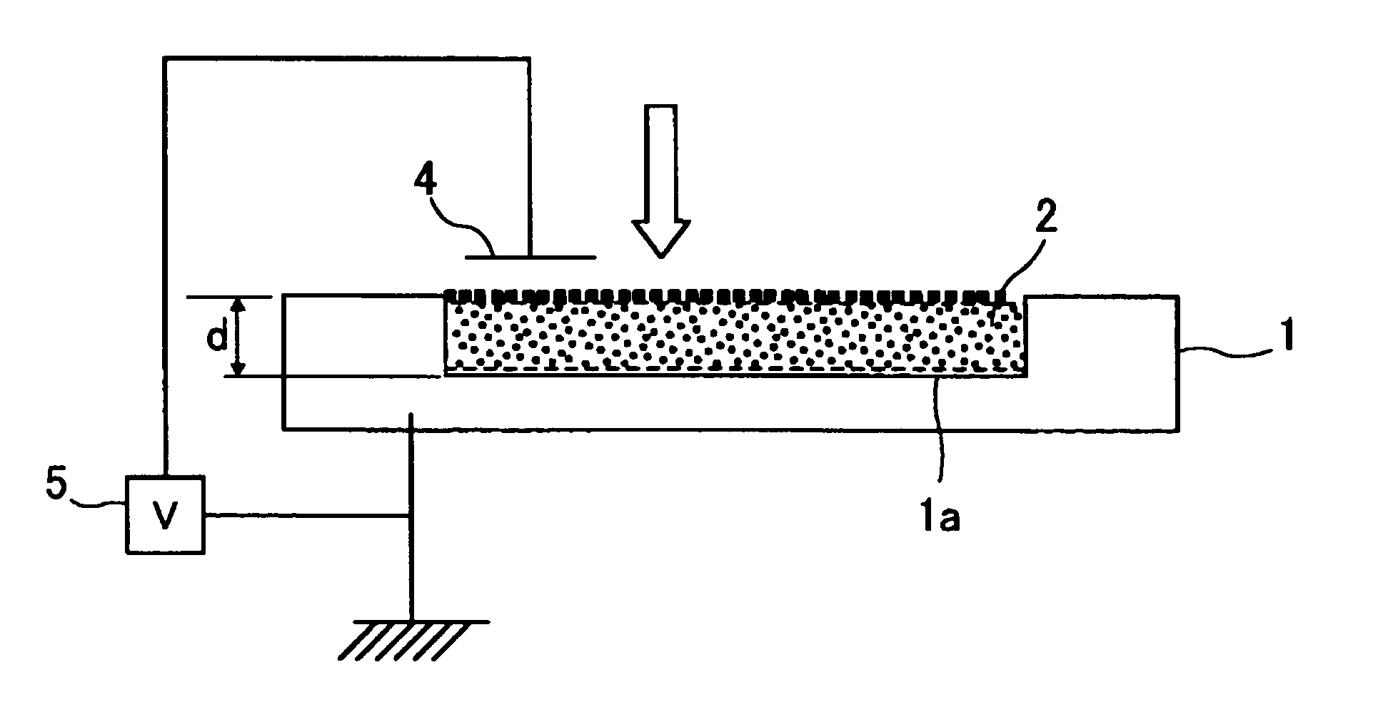
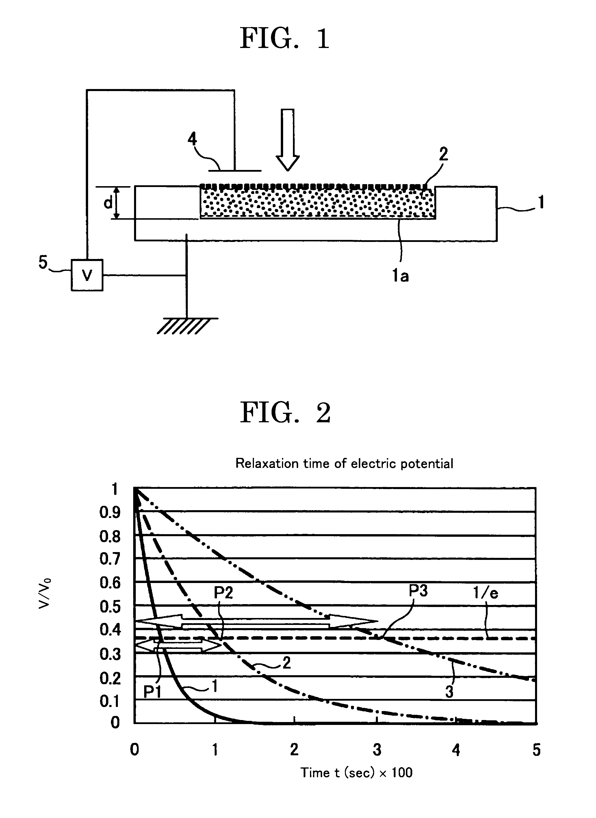
[0024]Specifically, the inventors of the present invention have found that the carriers of the present invention, in which a coating layer is formed on a core material surface, have different relaxation times, even though the carriers have the same physical properties such as carrier resistance, and that the carrier adhesion can be significantly prevented by controlling the relaxation time. Specifically, in the carrier of the present invention, an electric resistance property which changes over time according to the charge amount remaining in the carrier, namely, the relaxation time is optimized, in addition to the static electric resistance.
[0025]The inventors of the present invention have found that the carrier used in a developing system, in which direct current bias is applied as a developing bias, is significantly effective to prevent carrier adhesion and background smear, and to improve image density.

Problems solved by technology

From the viewpoint of developing process, making developing gap closely contacted, making a thin layer for a photoconductor, and making smaller diameter of a writing beam diameter, etc. are effective, however, these solutions still leave problems in terms of high-cost and reliability.
For example, Japanese Patent Application Laid-Open (JP-A) No. 58-144839 proposes a magnetic carrier containing ferrite particles having a spinel structure and an average particle diameter of 30 μm or less, however, the proposed carrier is not coated with a resin and is used under low-electric field, and is disadvantages in that it is poor developing ability, and the operating life is short.
However, the each of the proposed carriers having smaller particle diameters as described in JP-B No. 3029180 has disadvantages in that carrier adhesion easily occurs, and it is difficult to put them into practical use because the carrier adhesion causes occurrences of photoconductor flaws and fixing roller flaws.
In particular, when a carrier having a weight average particle diameter of less than 45 μm is used, the carrier surface smoothness is drastically improved, and a high quality image can be obtained, however, there are problems that carrier adhesion occurs very easily, and a high-quality image cannot be maintained over a long period of time.
Because the surface area per unit weight is large (large specific surface area) in the carrier particles having small diameters, the carrier particles having small diameters do not easily release charge, compared to carrier particles having large diameters.
Particularly, carrier adhesion caused by counter-charge, i.e. reverse-charge has been a big problem for the carrier having a small diameter.
However, as it stands, it is difficult to drastically change the parameters because the force closely relates to developing ability, background smear, toner scattering, and the like.

Method used


Image

  • Carrier, developer and electrophotographic developing method and image forming method
  • Carrier, developer and electrophotographic developing method and image forming method
  • Carrier, developer and electrophotographic developing method and image forming method

Examples


examples

[0145]Hereafter, the present invention will be further described in detail referring to specific examples, however, the present invention is not limited to the disclosed examples. It should be noted that “part” or “parts” represents “part by weight” or “parts by weight”, and “%” represents “% by weight”.

—Preparation of Toner—

[0146]

Polyester resin 100 partsQuinacridone magenta pigment 3.5 partsFluorine-containing quaternary ammonium salt  4 parts

[0147]The compositions described above were sufficiently mixed by a blender, and the mixture was melted and kneaded by a biaxial extruder. The kneaded product was cooled, and then coarsely crushed by a cutter mill. Next, the coarsely crushed product was finely pulverized in a jet stream pulverizer, and then classified by an air classifier to obtain toner base particles having a weight average particle diameter of 5.8 μm and a true specific gravity of 1.20.

[0148]Next, to 100 parts of the obtained toner base particles, 1.5 parts of hydrophobize...

example 1

[0167]To 100 parts of Carrier A (20), 13.1 parts of a toner was added, and stirred by a ball mill for 5 minutes to produce a developer having a toner content of 11.6% by weight. The toner coverage on the carrier was 50%.


PUM


Abstract

An object of the present invention is to provide a carrier containing core material particles having magnetism and a coating layer on the surfaces of the core material particles, wherein the core material particles have a magnetization at a magnetic field of 1,000 Oersted of 40 emu / g to 100 emu / g, and the carrier has a weight average particle diameter of 20 μm to 45 μm, a resistance (LogR) of 11 Ω·cm to 17 Ω·cm and a relaxation time τ of 150 seconds to 800 seconds.

Description

BACKGROUND OF THE INVENTION[0001]1. Field of the Invention[0002]The present invention relates to a carrier containing core material particles having magnetism and a coating layer on the surfaces of the core material particles, and also relates to a developer containing the carrier, an electrophotographic developing method and an image forming method using the developer.[0003]2. Description of the Related Art[0004]A developing process of electrophotography is classified into a one-component developing process using a one-component developer containing a toner, and a two-component developing process using a two-component developer containing glass beads, a magnetic carrier, or a coated carrier in which the surface of the glass beads or magnetic carrier are coated with a resin, and a toner.[0005]The charge characteristics is more stable in the two-component developing process than in the one-component developing process, because the carrier has a larger frictionally charged area. Thus,...

Claims


Application Information

Patent Timeline
IPC IPC(8): G03G9/083G03G13/04
CPCG03G9/0823G03G9/10G03G9/1139G03G9/1136G03G9/1075
Inventor YAMAGUCHI, KIMITOSHIIMAHASHI, NAOKISUZUKI, KOUSUKE
Owner RICOH KK
Learn More