Method and apparatus for manufacturing a semiconductor device

Inactive Publication Date: 2008-09-18
LONGITUDE SEMICON S A R L +1
View PDF6 Cites 0 Cited by
  • Summary
  • Abstract
  • Description
  • Claims
  • Application Information

AI Technical Summary

Benefits of technology

[0016]An object of the present invention is to provide a method and an apparatus for manufacturing a semiconductor device capable of solving any one of the problems conceivable in the above-described related arts that may occur. Another object of the present invention is to provide a method and an apparatus which do not require setting etching conditions allowing excessive margins in high-aspect ratio contact etching that is used in ULSI manufacturing and which can prevent the occurrence of etch-stop even if the chamber state changes while the best etching conditions remain unchanged during mass production.
[0017]In one aspect of the present invention, there is provided a method of manufacturing a semiconductor device wherein etching is performed on films on a wafer using a plasma treatment apparatus. In particular, there is provided a manufacturing method in which a change in the difference between the emission intensities of a first wavelength component and a second wavelength component in plasma is monitored during etching and, if the amount of change in the difference per unit time exceeds a predetermined threshold a given number of times in a row, then the flow rate of oxygen introduced to the plasma treatment apparatus is increased or, if the amount of change no longer exceeds the predetermined threshold, then the oxygen flow rate is set back to the original value thereof. As a result, it is possible to prevent the occurrence of etch-stop while keeping the best etching performance as is, thereby solving the above-described problem.

Problems solved by technology

The first case is a phenomenon in which the amount of seed depositions is excessively larger than the amount of ions contributing to etching and, therefore, the taper angle of a hole becomes large, which causes the hole to fail to penetrate through a film to-be-etched and which causes the hole's leading end to close.
If such an etch-stop, as described above occurs all over the wafer plane, all of the devices formed on the wafer become defective.
In the case of insulating film etching, etch-stop occurs mostly due to the above-described first case wherein the amount of seed depositions in plasma becomes excessively large.
However, etch-stop due to the above-described second case infrequently occurs just because etching slightly deviates from favorable etching conditions.
The most important of these requirements is “no etch-stop.” This is because the occurrence of etch-stop directly leads to a yield decrease, thereby causing a serious problem.
Therefore, it becomes less easy to secure etching conditions allowing margins at the time of mass production since the performance (specifications) required for etching becomes severer along with the advance in device miniaturization.
However, this document does not describe at all the steps that need to be taken after etch-stop is avoided.
If the additive amount of O2 that increased from the start of etching remains unchanged after the avoidance of etch-stop, it may become no longer possible to satisfy the specifications required for contact etching, including the etching rate, the selectivity to mask, the selectivity to substrate, the dimensional shift, and the amount of bowing.
However, this method requires that the flow rates of various gases be controlled in order to always maintain the emission intensities of C, F and O in plasma within correct ranges, thereby causing control configuration to become complicated.

Method used


Image

  • Method and apparatus for manufacturing a semiconductor device
  • Method and apparatus for manufacturing a semiconductor device
  • Method and apparatus for manufacturing a semiconductor device

Examples


Embodiment Construction

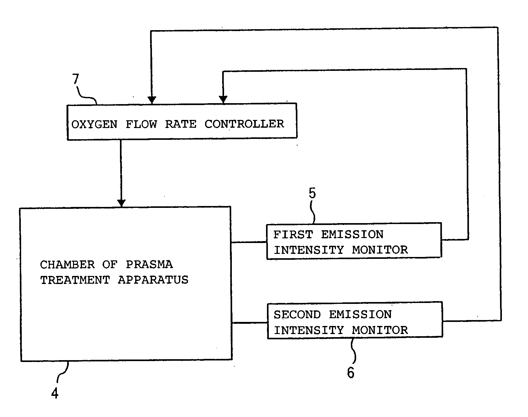
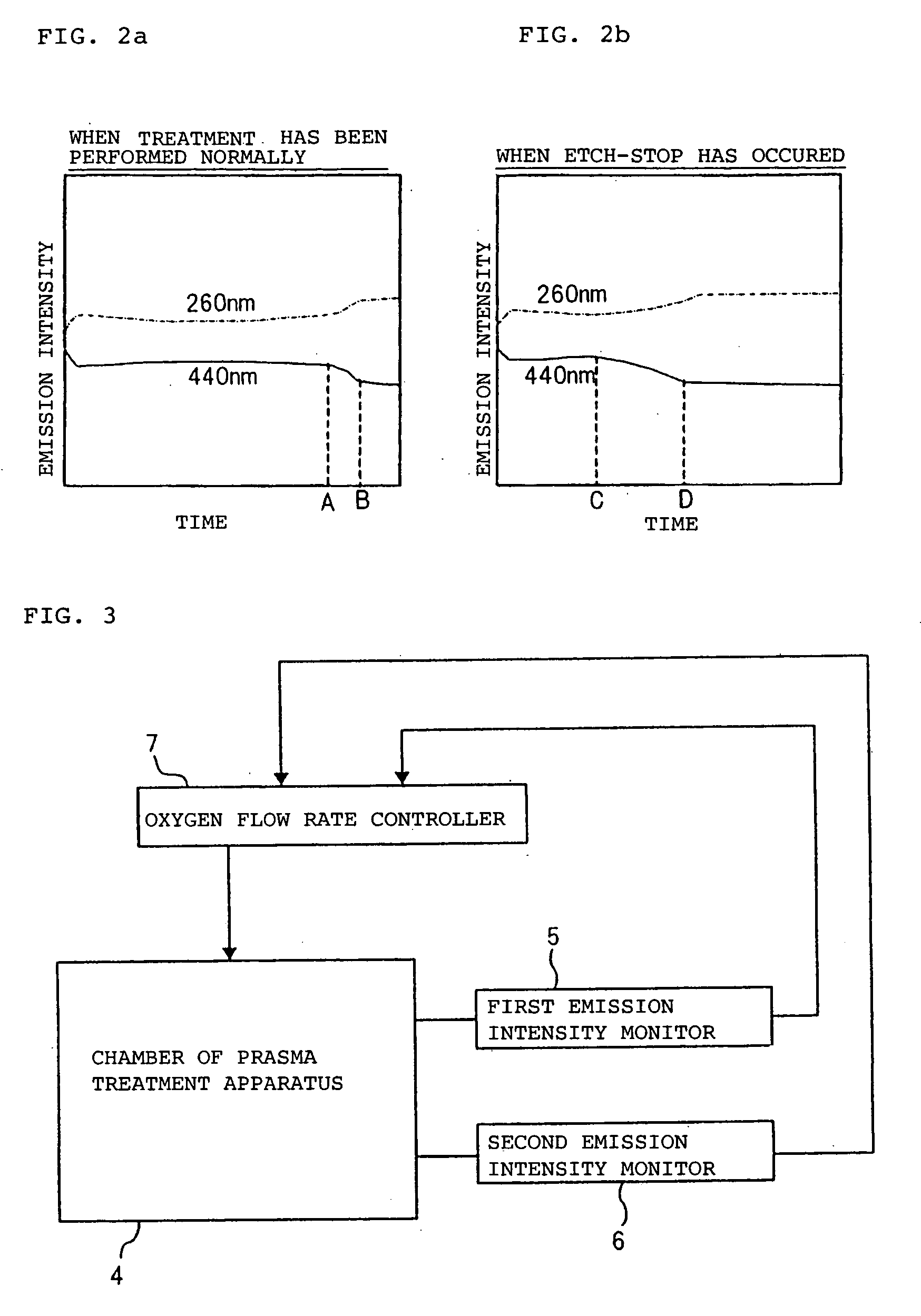
[0028]The exemplary embodiments of the present invention are based on the mechanism of the occurrence of etch-stop described in detail hereinafter. As described in the Related Art section, there are two cases in which etch-stop occurs. The first case is that etch-stop occurs because the amount of seed depositions in plasma becomes excessively large, as described in the Related Art section. On the other hand, the second case of etch-stop occurs when several conditions coincide. Here, consideration will be made in particular to the mechanism of the occurrence of the second case.

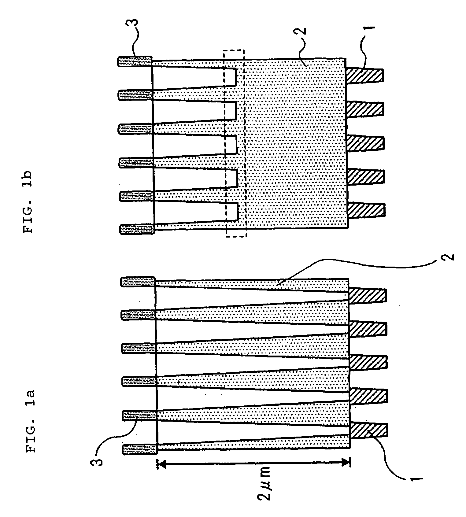
[0029]FIG. 1 is a schematic view in which a cross-sectional shape is compared between a case in which treatment has been performed normally in contact etching (FIG. 1a) and a case in which etch-stop has occurred (FIG. 1b). In this figure, contact plugs 1 (material: poly-Si) that are to be connected to transistors are formed on the surface layer of a silicon wafer, and film 2 (material: SiO2) that is to be etche...


PUM

PropertyMeasurementUnit
Wavelengthaaaaaaaaaa
Timeaaaaaaaaaa

Abstract

The present invention relates to a method of manufacturing a semiconductor device wherein etching is performed on films on a wafer using a plasma treatment apparatus. In the manufacturing method according to the present invention, a change in the difference between the emission intensities of a first wavelength component and a second wavelength component in plasma is monitored during etching. If the amount of change in the difference per unit time exceeds a predetermined threshold a given number of times in a row, then the flow rate of oxygen introduced to the plasma treatment apparatus is increased or, if the amount of change exceeding the predetermined threshold has not been seen, then the oxygen flow rate is set back to the original value thereof. This series of actions is repeated all the time during a set period of time.

Description

[0001]This application is based upon and claims the benefit of priority from Japanese patent application No. 2007-051407, filed on Mar. 1, 2007, the disclosure of which is incorporated herein in its entirety by reference.BACKGROUND OF THE INVENTION[0002]1. Field of the Invention[0003]The present invention relates to a method and an apparatus used in a process of dry-etching films on a wafer to form contact holes, including via holes and through holes, (hereinafter referred to as contact etching) in the manufacture of semiconductor devices, such as ULSIs.[0004]2. Description of the Related Art[0005]As one of the most fearful failures in contact etching, there is mentioned “etch-stop.” Etch-stop refers to a phenomenon in which etching stops while in progress.[0006]Etch-stop can be roughly classified into two cases. The first case is a phenomenon in which the amount of seed depositions is excessively larger than the amount of ions contributing to etching and, therefore, the taper angle...

Claims


Application Information

Patent Timeline
IPC IPC(8): H01L21/66H01L21/306C23F1/00
CPCH01J37/32935H01L22/20H01J37/32972
Inventor UEDA, YASUHIKO
Owner LONGITUDE SEMICON S A R L
Why Eureka
Try Eureka