Method for determining best and worst cases for interconnects in timing analysis

a timing analysis and interconnection technology, applied in the direction of individual semiconductor device testing, semiconductor/solid-state device testing/measurement, instruments, etc., can solve the problems of product yield at increasing risk, product may fail timing, and uncertainty in propagation tim

Active Publication Date: 2008-09-18
SYNOPSYS INC
View PDF10 Cites 19 Cited by
  • Summary
  • Abstract
  • Description
  • Claims
  • Application Information

AI Technical Summary

Benefits of technology

[0008]According to the invention, roughly described, minimum and / or maximum signal propagation delay values are estimated for each of a plurality of interconnects in a circuit design. For each particular interconnect, the propagation delay value(s) are estimated in dependence upon a preliminary approximate determination of whether the signal propagation delay is dominated more by an interconnect capacitance term or by an interconnect capacitance and resistance product term. If it is dominated more by the interconnect capacitance term, then the parameter values used for the minimum propagation delay calculation are obtained assuming a smallest capacitance process variation case and the parameter values used for the maximum propagation delay calculation are obtained assuming a largest capacitance process variation case. If the signal propagation delay is dominated more by the interconnect capacitance and resistance product term, then the parameter values used for the minimum propagation delay calculation are obtained assuming the largest capacitance process variation case and the parameter values used for the maximum propagation delay calculation are obtained assuming the smallest capacitance process variation case.

Problems solved by technology

Product yield is at increasing risk unless process variations and their impacts are properly modeled in the simulations.
The values of R and C for an interconnect largely determine the signal propagation time from a source node to a destination node, so the uncertainty in R and C results in uncertainty in the propagation time.
A product therefore may fail in timing if the large uncertainty in R and C is not properly taken into account when calculating propagation delays.
One cannot determine these absolutely, of course, because there will always be a small possibility of particular set of conditions in which signals propagate slightly faster or slightly more slowly.
This practice may give rise to misleading results for two reasons.
First, R and C variations are often correlated: a particular interconnect that turns out on fabrication to exhibit better capacitance performance, also tends to exhibit worse resistance performance, and vice-versa.
Furthermore, it can be seen that if the entire design is analyzed using “best case” capacitances, conditions may be such that one individual interconnect may exhibit the shortest propagation delay while another individual interconnect may exhibit the longest propagation delay.
If the two interconnects happen to be in the same delay path (e.g. in a chain of several drivers interconnected by metal wires), one would not be able to assert whether the overall path delay is the shortest or longest.
Consequently, one does not know whether the delay path satisfies the timing requirements for the design to meet product specifications.

Method used


Image

  • Method for determining best and worst cases for interconnects in timing analysis
  • Method for determining best and worst cases for interconnects in timing analysis
  • Method for determining best and worst cases for interconnects in timing analysis

Examples


Embodiment Construction

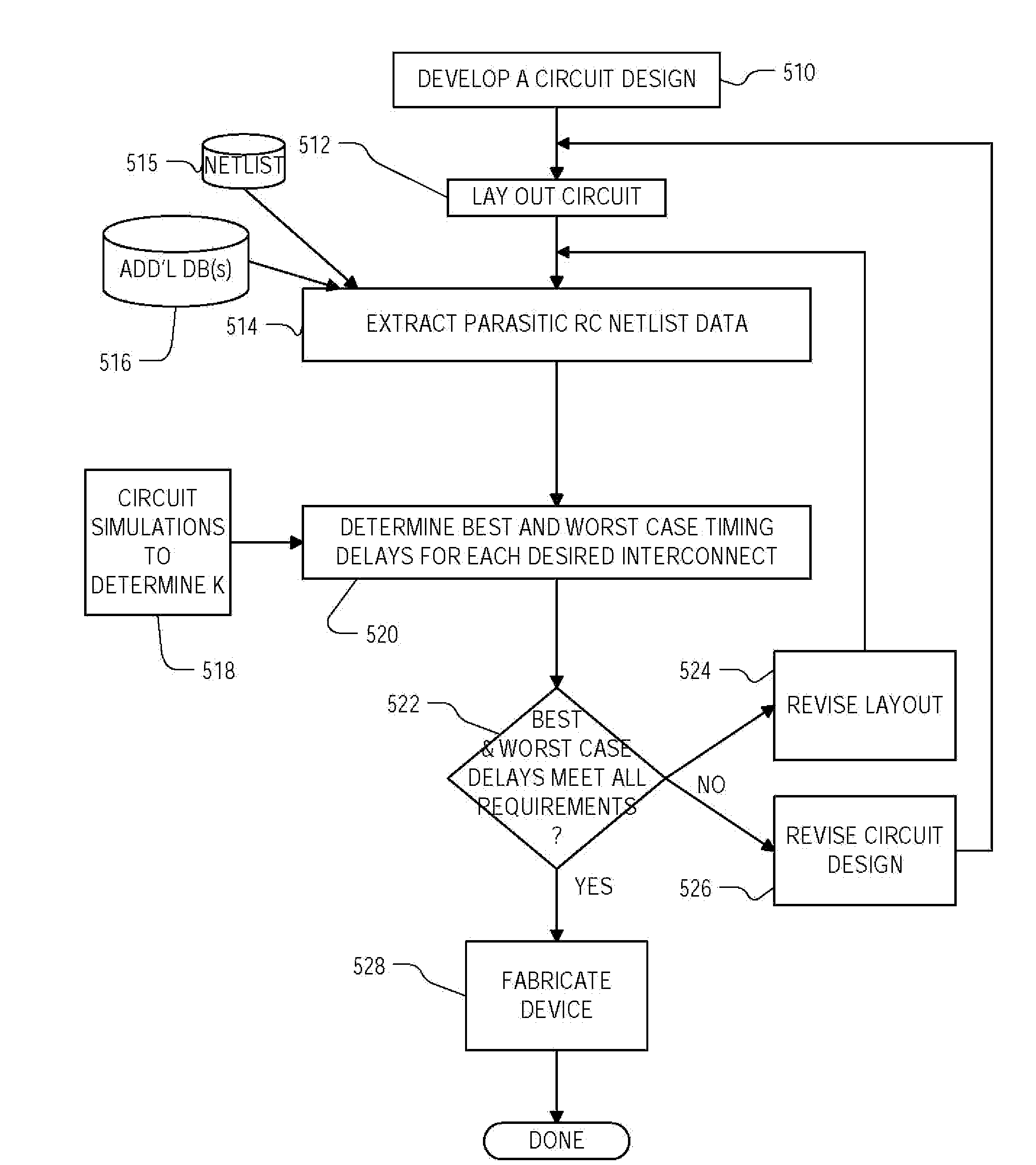
[0022]The following detailed description is made with reference to the figures. Preferred embodiments are described to illustrate the present invention, not to limit its scope, which is defined by the claims. Those of ordinary skill in the art will recognize a variety of equivalent variations on the description that follows.

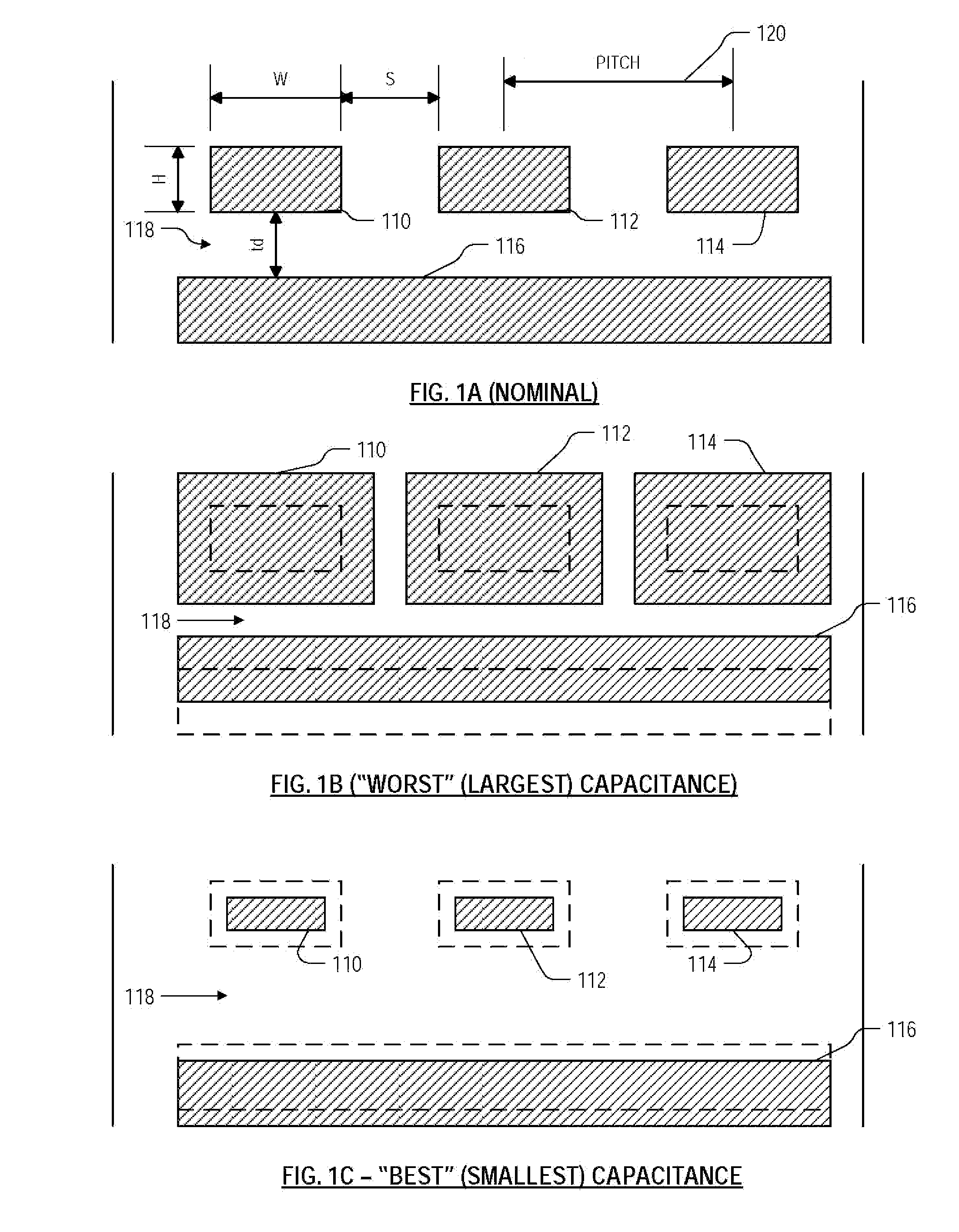
[0023]FIG. 1A is a symbolic diagram of a portion of an integrated circuit device. Shown are three metal conductors 110, 112 and 114, extending into the plane of the page and viewed in cross-section, and a fourth conductor or ground plane 116 located in a layer below and separated by a dielectric layer 118. For this illustration, the conductors 110, 112 and 114 have a pitch 120. They all have a width W, a thickness H, and are spaced from each other by a distance S. The conductors 110, 112 and 114 are all separated from the underlying layer 116 by spacing td. FIG. 1A may illustrate the geometric characteristics of a device fabricated exactly as specified in the lay...


PUM


Abstract

Roughly described, signal propagation delay values are estimated for a plurality of interconnects in a circuit design. For each interconnect, the propagation delay value(s) are estimated in dependence upon a preliminary approximate determination of whether the signal propagation delay is dominated more by an interconnect capacitance term or by an interconnect capacitance and resistance product term. If it is dominated more by the interconnect capacitance term, then the parameter values used for a minimum propagation delay calculation are obtained assuming a smallest capacitance process variation case and the parameter values used for a maximum propagation delay calculation are obtained assuming a largest capacitance process variation case. If the signal propagation delay is dominated more by the interconnect capacitance and resistance product term, then the opposite assumptions are made. Preferably the approximate determination is made by comparing Rint to k*Rd.

Description

BACKGROUND[0001]The present invention relates to integrated circuit simulation technology, and more particularly to analysis of the timing of signal propagation.[0002]Because of the long time required and the large expense involved for fabricating test versions of integrated circuits, it has become commonplace to simulate the operation of circuit designs as thoroughly as possible before fabricating a prototype. In this way corrections can be made before the time and expense of prototype fabrication is incurred. One parameter that is typically tested in these simulations is the propagation delay, from the output of a source node to the input of a destination node. Typically it is required that the propagation time must be short enough such that when added to the setup time requirement of the destination node, a signal asserted at the source node will reach the destination node soon enough to be stable when required by the destination node. The propagation time also must be long enoug...

Claims


Application Information

Patent Timeline
Patent Type & Authority Applications(United States)
IPC IPC(8): G06F17/50
CPCG06F2217/84G06F17/5031G06F30/3312G06F2119/12
Inventor LIN, XI-WEIPRAMANIK, DIPANKAR
Owner SYNOPSYS INC
Why Eureka
Try Eureka