Image sensor, single-plate color image sensor, and electronic device

a color image sensor and image sensor technology, applied in the field of image sensors, can solve the problems of affecting the spectral sensitivity the use of the avalanche multiplication layer is not necessarily suitable for miniaturization of the pixel, and the inability to avoid the tendency of decreasing the sensitivity of the image sensor, etc., to achieve the effect of suppressing the decrease of sensitivity and the change of spectral sensitivity

Inactive Publication Date: 2008-09-25
KK TOSHIBA
View PDF9 Cites 21 Cited by
  • Summary
  • Abstract
  • Description
  • Claims
  • Application Information

AI Technical Summary

Benefits of technology

[0014]It is an object of the present invention to provide an image sensor, which is capable of suppressing a decrease of sensitivity and change of spectral sensitivity.

Problems solved by technology

In association with the miniaturization of the pixel, it is impossible to avoid a tendency of decreased sensitivity of the image sensors.
Thus, the use of the avalanche multiplication layer is not necessarily suitable for miniaturization of the pixel.
Thus, there is a problem in that a spectral sensitivity of the avalanche multiplication layer is changed.

Method used


Image

  • Image sensor, single-plate color image sensor, and electronic device
  • Image sensor, single-plate color image sensor, and electronic device
  • Image sensor, single-plate color image sensor, and electronic device

Examples


first embodiment

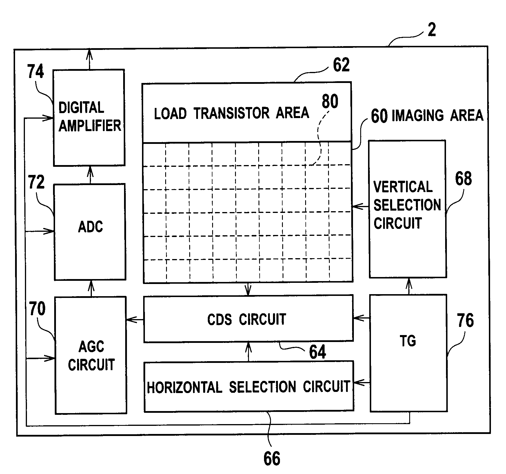
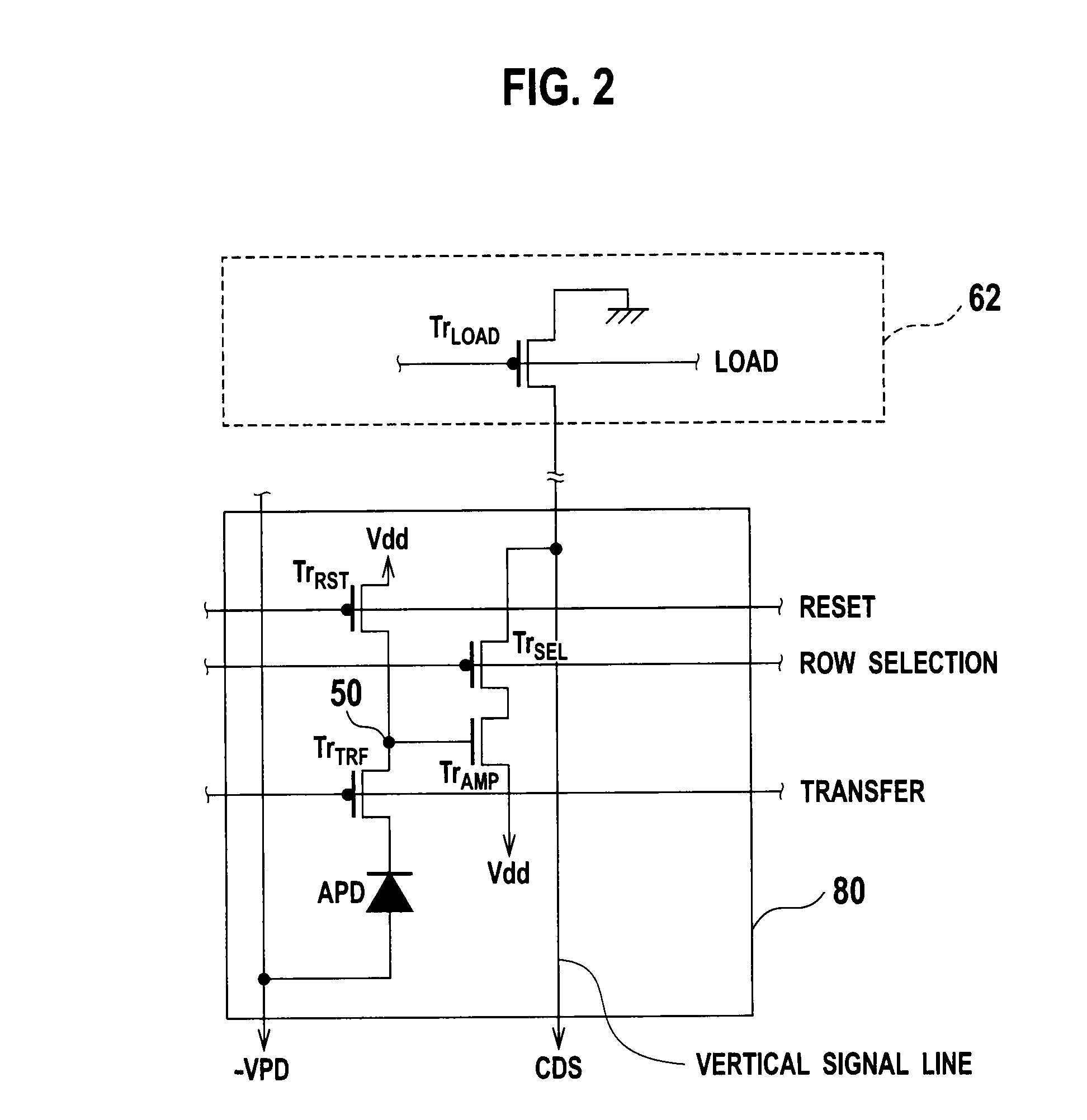
[0036]An image sensor 2 according to a first embodiment of the present invention includes an imaging area 60, a load transistor area 62, a correlated double sampling (CDS) circuit 64, a horizontal selection circuit 66, a vertical selection circuit 68, an automatic gain control (AGC) circuit 70, an analog-digital converter (ADC) 72, a digital amplifier 74 and a timing generator (TG) 76. The imaging area 60 includes a plurality of cells 80, arrayed in a matrix. Each of the plurality of cells 80 functions as a pixel and converts a signal charge, generated from an incident light signal by photoelectric conversion, to a voltage so as to generate an analog signal. The load transistor area 62 is arranged in contact with the imaging area 60. The load transistor area 62 includes a source follower circuit provided in combination with an amplifying transistor of a pixel selected by the vertical selection circuit 68, so as to transmit the analog signal voltage, which is generated by each pixel,...

second embodiment

[0073]A single-plate color image sensor according to a second embodiment of the present invention includes a cell 80 in which four pixels 4a, 4b and 4c are arranged as a Bayer array, as shown in FIG. 11. The pixel 4a is used for blue color (B). Two pixels 4b are used for blue and green colors (B+G). The pixel 4c is used for blue, green and red color (B+G+R).

[0074]The pixel 4a includes a first avalanche photodiode (12a, 13a and 14a) and a first transfer transistor (16A, 22A and 16B), as shown in FIG. 12. The first avalanche photodiode (12a, 13a and 14a) includes a first anode region 12a, a first avalanche multiplication region 13a and a first cathode region 14a. The first anode region 12a and the first cathode region 14a have substantially the same depth Da. The first transfer transistor (16A, 22A and 16B) includes a first source region 16A, a first gate electrode 22A and a first drain region 16B. The first source region 16A is electrically connected to the first cathode region 14a t...


PUM


Abstract

An image sensor includes an imaging area including a plurality of cells arrayed in a matrix on a semiconductor substrate, each of the cells including an avalanche photodiode, the avalanche photodiode including: an anode region buried in an upper portion of the semiconductor substrate; a cathode region buried in the upper portion of the semiconductor substrate separated from the anode region in a direction parallel to the surface of the semiconductor substrate; and an avalanche multiplication region defined between the anode and cathode regions, the avalanche multiplication region having an impurity concentration less than the anode and cathode regions; wherein depths of the anode and cathode regions from the surface of the semiconductor substrate are different from each other.

Description

CROSS REFERENCE TO RELATED APPLICATIONS AND INCORPORATION BY REFERENCE[0001]This application is based upon and claims the benefit of priority from prior Japanese patent application P2007-074879 filed on Mar. 22, 2007; the entire contents of which are incorporated by reference herein.BACKGROUND OF THE INVENTION[0002]1. Field of the Invention[0003]The present invention relates to an image sensor, and particularly to an image sensor using an avalanche photodiode, a single-plate color image sensor and an electronic device.[0004]2. Description of the Related Art[0005]With an increase in the market of electronic devices, such as digital cameras, portable telephones with a built-in camera, and the like, the development of image sensors is being actively pursued. In particular, there is intensified competition in the development of a metal-oxide semiconductor (MOS) image sensor, which can be manufactured by typical semiconductor manufacturing processes, such as complementary MOS (CMOS) proc...

Claims


Application Information

Patent Timeline
Patent Type & Authority Applications(United States)
IPC IPC(8): H04N5/335H01L27/146H04N5/369H04N5/372H04N5/374H04N5/376H04N9/07
CPCH01L27/14603H01L31/0352H01L27/14645H01L27/1461
Inventor IIDA, YOSHINORI
Owner KK TOSHIBA
Why Eureka
Try Eureka