Interconnect Structures for Semiconductor Devices

a technology of interconnect structure and semiconductor device, which is applied in the direction of semiconductor device, semiconductor/solid-state device details, electrical apparatus, etc., can solve the problems of rc yield loss, metal residue on the surface of the ild layer, easy oxidation of copper,

Inactive Publication Date: 2008-09-25
TAIWAN SEMICON MFG CO LTD
View PDF12 Cites 31 Cited by
  • Summary
  • Abstract
  • Description
  • Claims
  • Application Information

AI Technical Summary

Benefits of technology

[0007]These and other problems are generally solved or circumvented, and technical advantages are generally achieved, by ...

Problems solved by technology

The change in the conductive line material and insulating materials of semiconductor devices has introduced new challenges in the manufacturing process.
For example, copper oxidizes easily and has a tendency to diffuse into adjacent insulating materials, particularly when a low-K material or other porous insulator is used for the ILD layer.
While the CoWP and C...

Method used


Image

  • Interconnect Structures for Semiconductor Devices
  • Interconnect Structures for Semiconductor Devices
  • Interconnect Structures for Semiconductor Devices

Examples


Embodiment Construction

[0015]The making and using of the presently preferred embodiments are discussed in detail below. It should be appreciated, however, that the present invention provides many applicable inventive concepts that can be embodied in a wide variety of specific contexts. The specific embodiments discussed are merely illustrative of specific ways to make and use the invention, and do not limit the scope of the invention.

[0016]The present invention will be described with respect to embodiments in a specific context, namely forming copper interconnects in an intermetal dielectric layer. The invention may also be applied, however, to other designs in which it is desirable to limit contamination between materials or to increase adhesive qualities of successive layers.

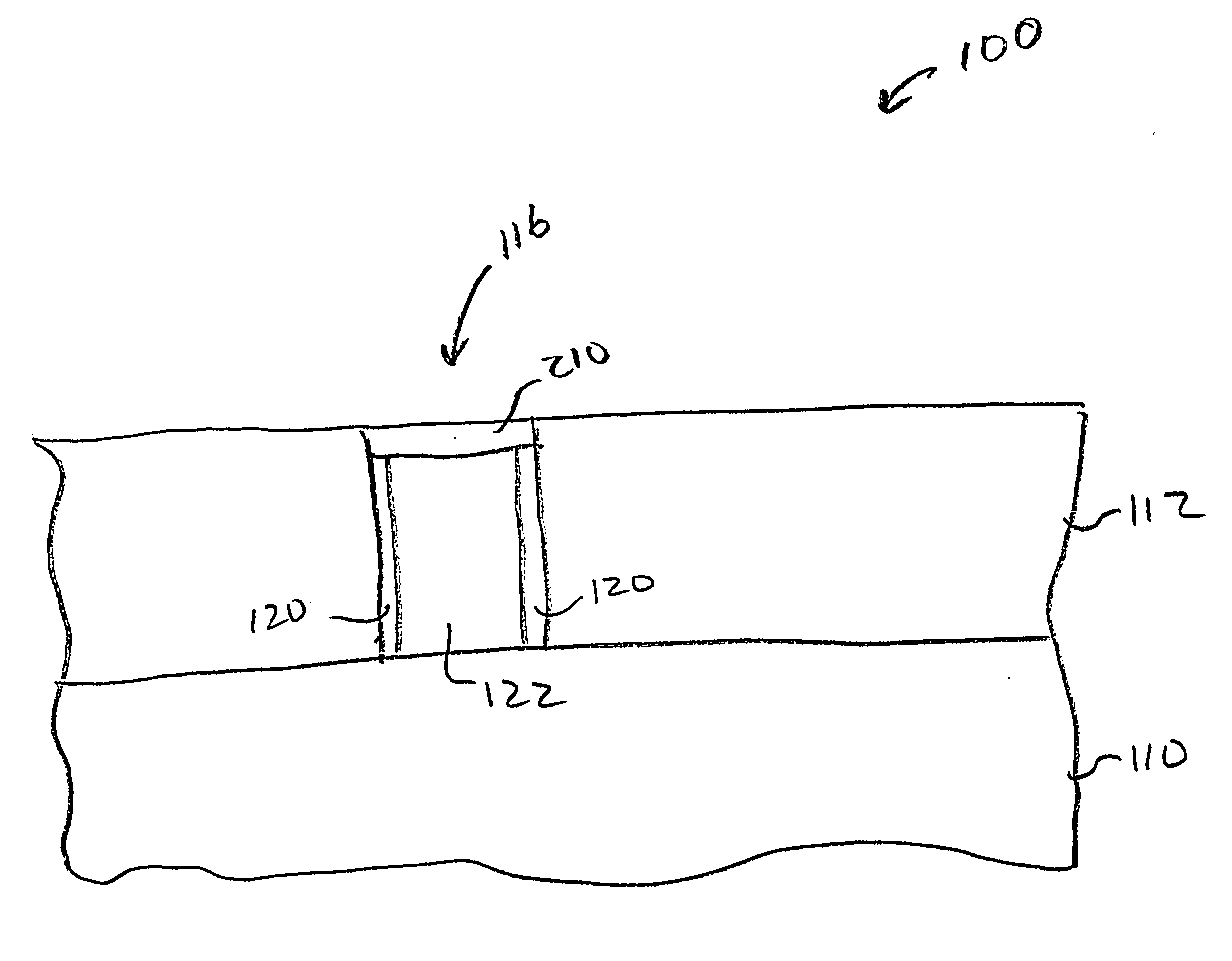
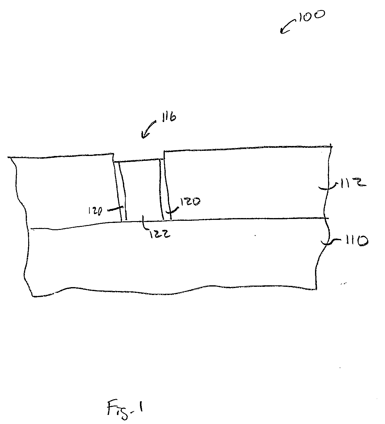
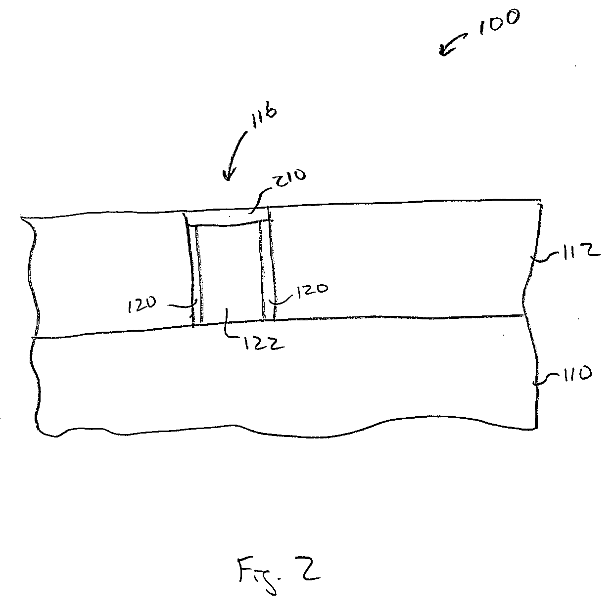
[0017]FIGS. 1-5 illustrate cross-section views of a first embodiment of the present invention in which a cap layer is formed on a metal layer. Referring first to FIG. 1, a workpiece 100 is provided. The workpiece 100 comprises a sem...


PUM


Abstract

A cap layer for a copper interconnect structure formed in a first dielectric layer is provided. In an embodiment, the cap layer may be formed by an in-situ deposition process in which a process gas comprising germanium, arsenic, tungsten, or gallium is introduced, thereby forming a copper-metal cap layer. In another embodiment, a copper-metal silicide cap is provided. In this embodiment, silane is introduced before, during, or after a process gas is introduced, the process gas comprising germanium, arsenic, tungsten, or gallium. Thereafter, an optional etch stop layer may be formed, and a second dielectric layer may be formed over the etch stop layer or the first dielectric layer.

Description

[0001]This application claims the benefit of U.S. Provisional Application No. 60 / 919,650, filed on Mar. 23, 2007, entitled “Cu-M / Cu-MSi Formation Using Si Seed Catalysts,” which application is hereby incorporated herein by reference.TECHNICAL FIELD[0002]The present invention relates generally to semiconductors and, more particularly, to a cap layer over a conductive layer in a semiconductor device.BACKGROUND[0003]Generally, integrated circuits (ICs) comprise electronic components, such as transistors, capacitors, or the like, formed on a substrate. One or more metal layers are then formed over the electronic components to provide connections between the electronic components and to provide connections to external devices. The metal layers typically comprise an inter-layer dielectric (ILD) layer in which interconnect structures, such as vias and conductive traces, are formed, usually with a single- or dual-damascene process.[0004]The trend in the semiconductor industry is towards the...

Claims


Application Information

Patent Timeline
IPC IPC(8): H01L21/441
CPCH01L21/28556H01L21/76834H01L21/76849H01L21/76867H01L21/76883H01L21/76877H01L21/76889H01L21/76843H01L21/32053H01L21/76802H01L21/76871H01L21/76886H01L2924/0002H01L2924/00H01L23/528H01L23/53233H01L23/53238
Inventor CHANG, HUI-LINTSAI, HUNG CHUNLU, YUNG-CHENGJANG, SYUN-MING
Owner TAIWAN SEMICON MFG CO LTD
Why Eureka
Try Eureka