Plasma Processing Apparatus

Inactive Publication Date: 2008-10-02
HITACHI HIGH-TECH CORP
View PDF4 Cites 147 Cited by
  • Summary
  • Abstract
  • Description
  • Claims
  • Application Information

AI Technical Summary

Benefits of technology

[0007]One object of this invention is to provide a plasma processing apparatus which can uniformly remove the adhesive substances deposited on the sample surface and therefore enjoy an improved process yield. Another object of this invention is to provide a plasma processing apparatus which can provid

Problems solved by technology

According to the conventional technique disclosed in JP-A-2005-277369, the change in the process condition causes the change in the thickness of the sheath formed above the sample, the shapes of the equipotential surfaces and the heights of the equipotential surfaces, with the result that the same capability of removing the adhesive substance as achieved before the process change can be no longer achieved with the same thickness of the insulating material when the electric field near around the periphery of the sample changes.
When it is necessary to change processing conditions depending on the sorts of layers, this conventional technique still suffers a problem that the adhesive substances deposited on the outer periphery of the sample cannot be satisfactorily removed.
Further, with

Method used


Image

  • Plasma Processing Apparatus
  • Plasma Processing Apparatus
  • Plasma Processing Apparatus

Examples


Example

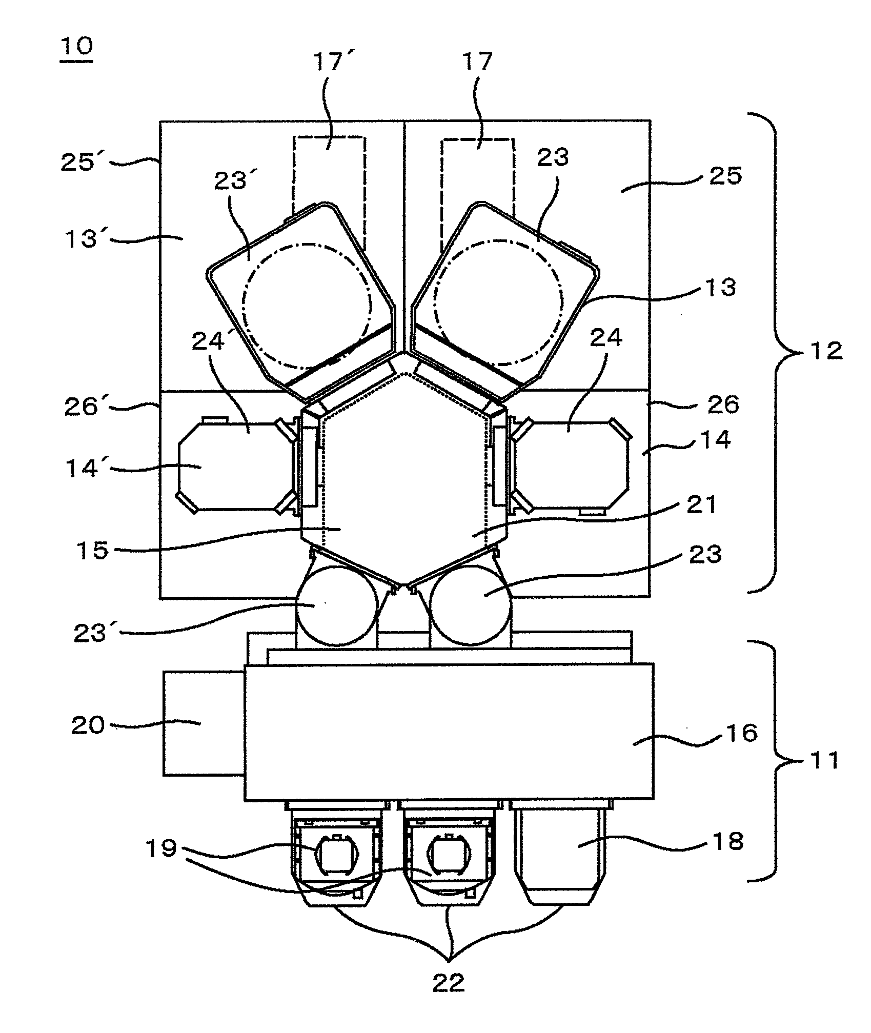
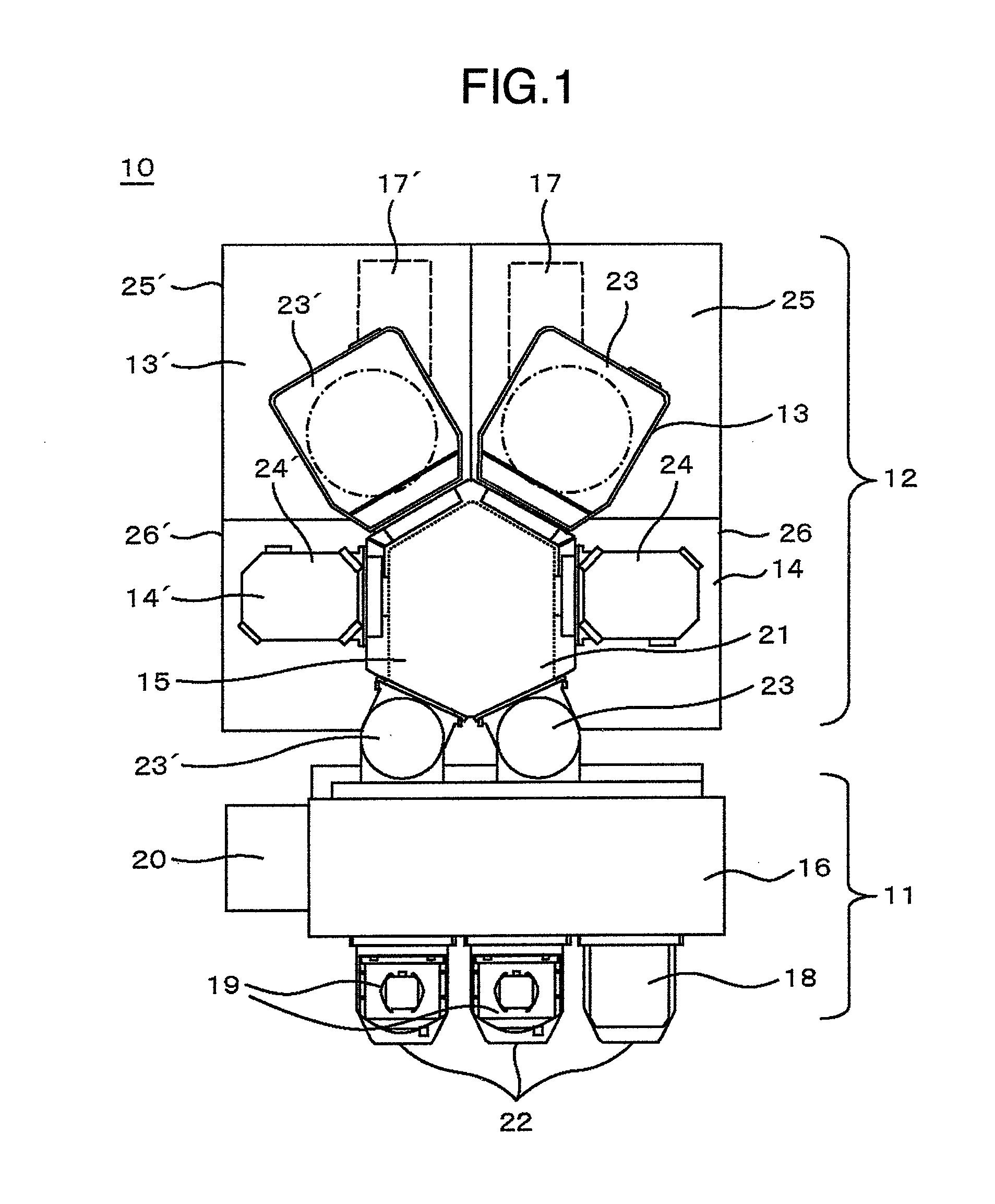
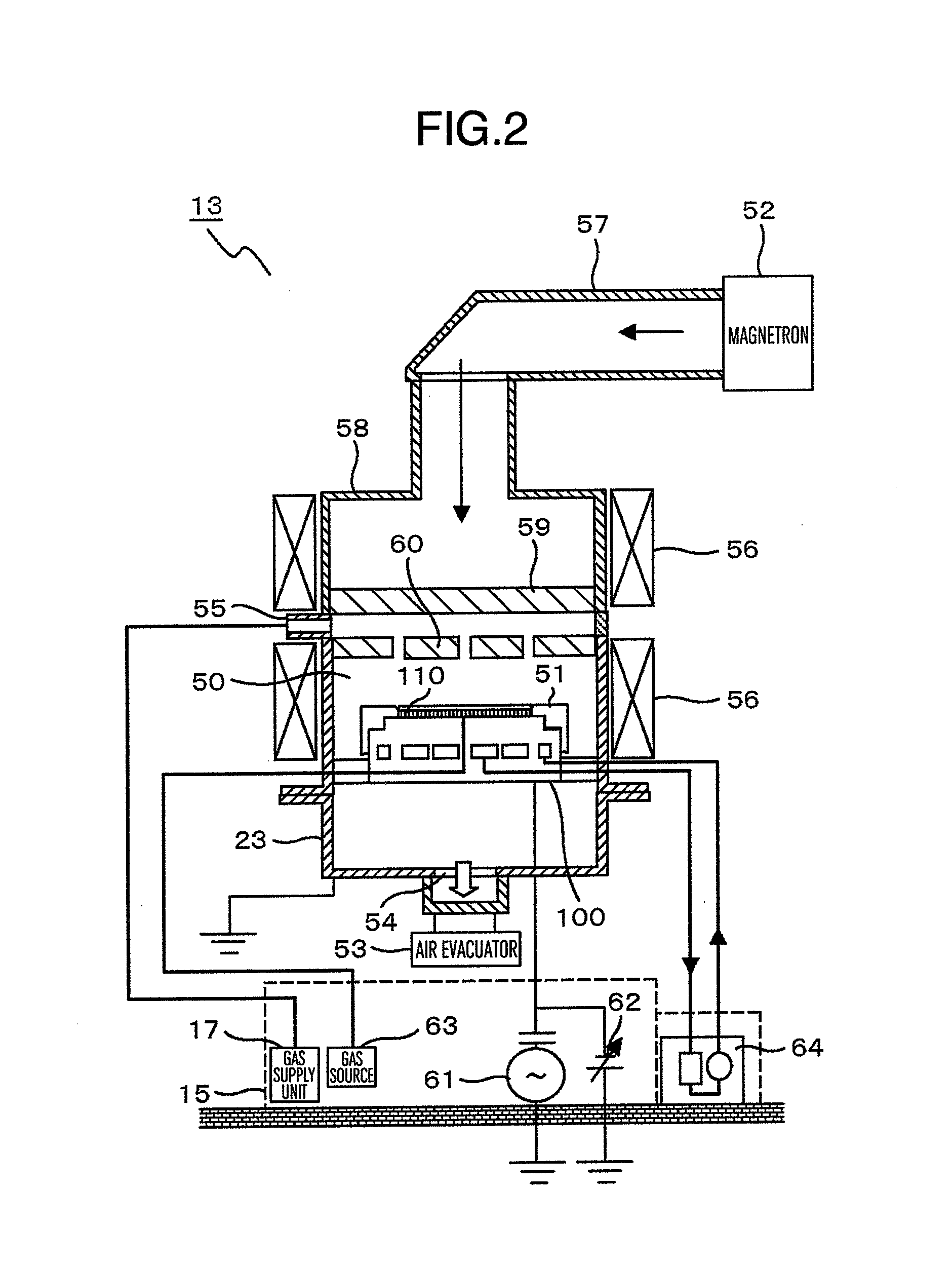
[0024]The first embodiment of this invention will be described with reference to FIGS. 1 through 7.

[0025]As shown in FIG. 1, a vacuum processing apparatus 10 according to this invention can be roughly divided into two blocks, front block and rear block. The front block, located near the bottom of FIG. 1, of the vacuum processing apparatus 10 is usually placed in a clean room and faces the conveyer line that carries the cassette encasing therein a semiconductor wafer as a sample substrate to be processed. Along the conveyer line are arranged plural vacuum processing apparatuses 10 and other processing apparatuses to form a so-called manufacturing line.

[0026]The front block is referred to as an atmospheric pressure block 11. For this block first receives a wafer under the atmospheric pressure before it is transferred into the depressurized chamber of the vacuum processing apparatus 10. The rear block, located near the top of FIG. 1, of the vacuum processing apparatus 10 is referred to...


PUM

PropertyMeasurementUnit
Poweraaaaaaaaaa
Diameteraaaaaaaaaa
Structureaaaaaaaaaa

Abstract

A plasma processing apparatus wherein a layer structure consisting of plural layers formed in stack one upon another on a semiconductor wafer placed on the sample holder located in the process chamber, is etched with plasma generated in the process chamber by supplying high frequency power to the electrode disposed in the sample holder, the apparatus comprising a ring-shaped electrode disposed above the electrode and around the periphery of the top portion of the sample holder, an outer circumferential ring of dielectric material disposed above the ring-shaped electrode and opposite to the plasma, and a power source for supplying power at different values to the ring-shaped electrode depending on the sorts of layers of the layer structure.

Description

BACKGROUND OF THE INVENTION[0001]This invention relates to a plasma processing apparatus wherein a sample in the form of a circular disk such as a semiconductor wafer is placed in the process chamber in the vacuum vessel and the sample is processed with plasma formed in the process chamber. It relates more particularly to a plasma processing apparatus wherein the sample is processed while it is being placed on the upper surface of the sample holder located in the depressurized process chamber.[0002]In such a plasma processing apparatus, the process gas fed into the process chamber to process the sample is excited by the electric or magnetic field developed in the process chamber so that plasma is formed, and then the chemical and / or physical interactions between the plasma particles and the material of the sample surface will allow at least one of the layers formed in the sample surface and supposed to be processed to be etched, for example. During this process, the process chamber ...

Claims


Application Information

Patent Timeline
IPC IPC(8): H01L21/306
CPCH01J37/32192H01J37/32568H01J37/32642H01L21/0273H01L21/31116H01L21/32137H01L21/32139
Inventor ARAMAKI, TOORUNISHIO, RYOJI
Owner HITACHI HIGH-TECH CORP
Why Eureka
Try Eureka