

Semiconductor device and manufacturing method of the same
a technology of semiconductor devices and manufacturing methods, applied in the direction of semiconductor devices, basic electric elements, electrical equipment, etc., can solve the problems of ohmic electrodes with low resistance are even more difficult to form, and the desired output cannot be obtained, etc., to achieve high breakdown voltage, high output, and high output.
- Summary
- Abstract
- Description
- Claims
- Application Information
AI Technical Summary
Benefits of technology
Problems solved by technology
Method used
Image

Examples
embodiment 1
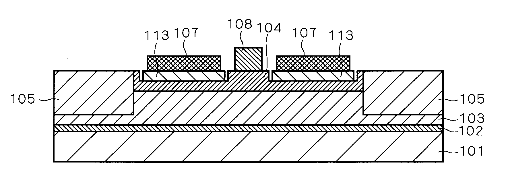
[0044]FIG. 1 is a cross-sectional drawing of the hetero-junction field effect transistor according to the embodiment of the present invention. In the hetero-junction field effect transistor shown in FIG. 1, a semi-insulated SiC substrate 1 is provided in the lowest layer, and a channel layer 3 of 1 μm thickness, consisting of Al0.6Ga0.4N, is provided on top of it via a buffer layer 2. Further, in the hetero-junction field effect transistor shown in FIG. 1, a barrier layer 4 of 10 nm thickness, consisting of AlN, forms a hetero-junction with the channel layer 3. Further, in the hetero-junction field effect transistor shown in FIG. 1, an element separation region 5 is provided in the regions on both sides in the drawing, and source / drain electrodes 6 consisting of Ti / Al and a gate electrode 7 consisting of Ni / Au are provided on the barrier layer 4.
[0045]The off breakdown voltage of the hetero-junction field effect transistor depends on the electric breakdown field of the channel layer...
embodiment 2
[0061]The calculation result of the energy band structure (energy (eV)) and the carrier concentration (cm−3) in the depth direction of the barrier layer 4 and the channel layer 3 of the hetero-junction field effect transistor shown in FIG. 1 is shown in FIG. 9. The calculation result is obtained by solving Poisson's equation and Schrödinger's equation self-consistently. Moreover, values that are generally used are used as physical property values used in the above-described calculation.
[0062]In the graph shown in FIG. 9, the value in which the carrier concentration is integrated with the depth direction is made to be the sheet carrier density (Ns), and the sheet carrier density of the hetero-junction field effect transistor shown in FIG. 1 is obtained to be 1.6×10¹³ (cm−2).
[0063]Similarly, the relationship of the sheet carrier density (cm−2) and the thickness (t) (nm) of the barrier layer 4 in the case of combining the Al composition ratio x of the channel layer 3 and the Al composi...
embodiment 3
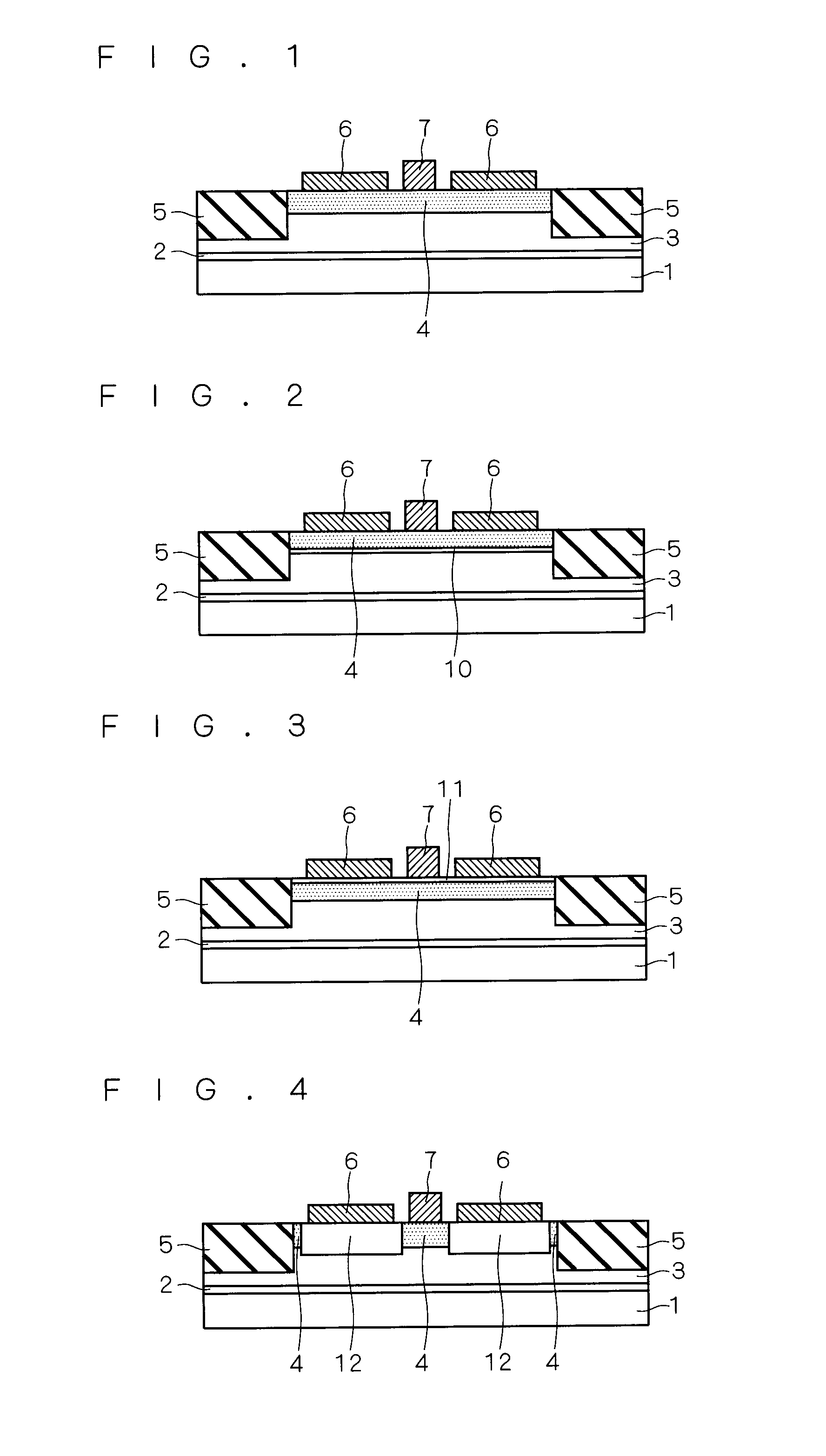
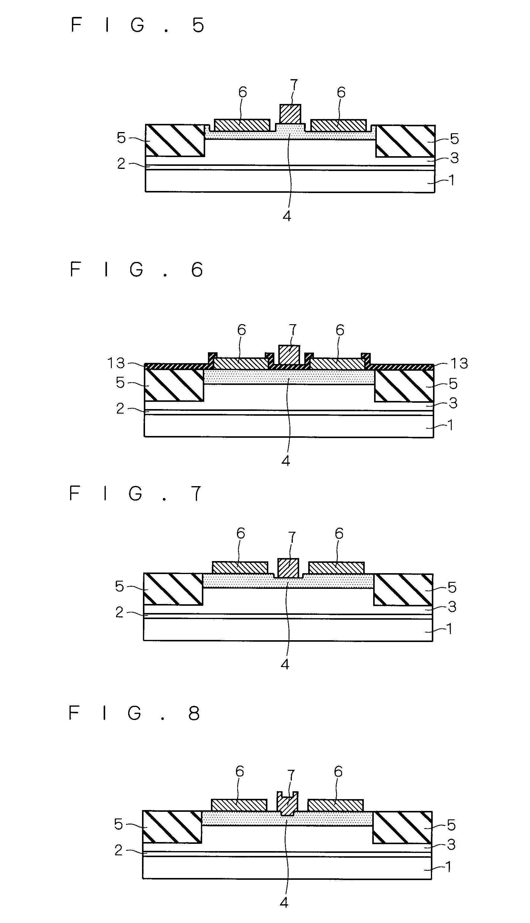
[0073]A manufacturing process of the hetero-j unction field effect transistor shown in FIG. 1 is shown in FIGS. 15 to 18. Moreover, the same reference numbers are appended to the constituting elements in FIGS. 15 to 18 that are the same constituting elements shown in FIG. 1, and detailed explanation is omitted. First, with respect to FIG. 15, the buffer layer 2, the channel layer 3 consisting of Al0.6Ga0.4N, and the barrier layer 4 consisting of AlN are epitaxial grown in order by applying an epitaxial growth method such as a MOCVD (Metal Organic Chemical Vapor Deposition) method and a MBE (Molecular Beam Epitaxy) method on the SiC substrate 1.
[0074]Next, with respect to FIG. 16, a metal layer such as Ti, Al, Ni, Ta, Au, Mo, and W is deposited by using a vapor deposition method or a sputter method, and the source / drain electrodes 6 are formed with a lift-off method, etc.
[0075]Next, with respect to FIG. 17, the element separation region 5 is formed in the channel layer 3 and the barr...
PUM
 Abstract
Description
Claims
Application Information