Spatially aware drive strength dependent die size independent combinatorial spare cell insertion manner and related system and method

a drive strength and die size technology, applied in the field of integrated circuits, can solve the problems of increasing the area of the chip, increasing the area of the design, and the spare cell area, and achieve the effects of increasing the cell count of the design, short cycle time, and increasing the chip area

Inactive Publication Date: 2008-10-02
STMICROELECTRONICS SRL
View PDF2 Cites 22 Cited by
  • Summary
  • Abstract
  • Description
  • Claims
  • Application Information

AI Technical Summary

Benefits of technology

[0031]In the prior art, the addition of any cell increases the cell count of the design and thus increases the area of the chip. Thus, the addition of spare cells increases the area of the design. However, during cell placement there are normally blank spaces left out due to various reasons leading to the utilization metric. The higher the congestion, the higher the utilization value. The utilization rate is never 100%. According to the design method of the present invention, combinational spare cells are inserted into the filler cells (blank spaces) based upon a drive strength algorithm. Thus, post-modification, the chip has unconnected combinational cells strewn throughout the chip in a specific, identifiable, pattern. The presence of such a pattern in an “all filler” or zero percent utilization region can be used to detect the usage of the present design method in any chip, or a portion thereof.

Problems solved by technology

In the prior art, the addition of any cell increases the cell count of the design and thus increases the area of the chip.
Thus, the addition of spare cells increases the area of the design.
However, during cell placement there are normally blank spaces left out due to various reasons leading to the utilization metric.

Method used


Image

  • Spatially aware drive strength dependent die size independent combinatorial spare cell insertion manner and related system and method
  • Spatially aware drive strength dependent die size independent combinatorial spare cell insertion manner and related system and method
  • Spatially aware drive strength dependent die size independent combinatorial spare cell insertion manner and related system and method

Examples


Embodiment Construction

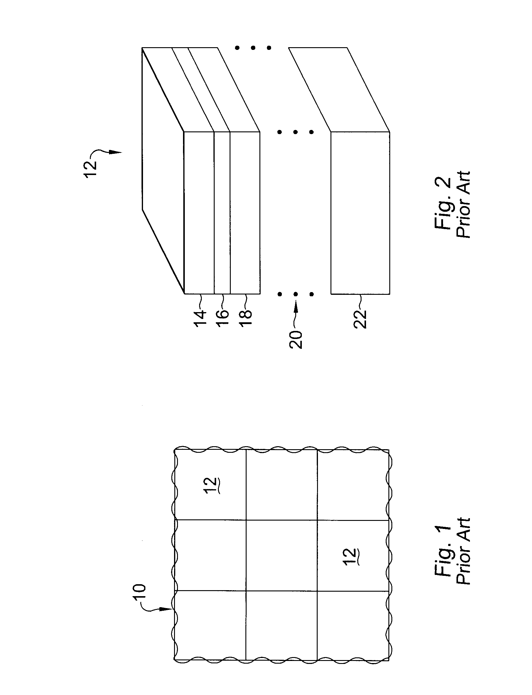
[0038]Although the following description uses the design of a semi-custom ASIC as an example, the description may also apply to full-custom ASICs, FPGAs, other programmable logic devices (PLD), and other ICs in general.

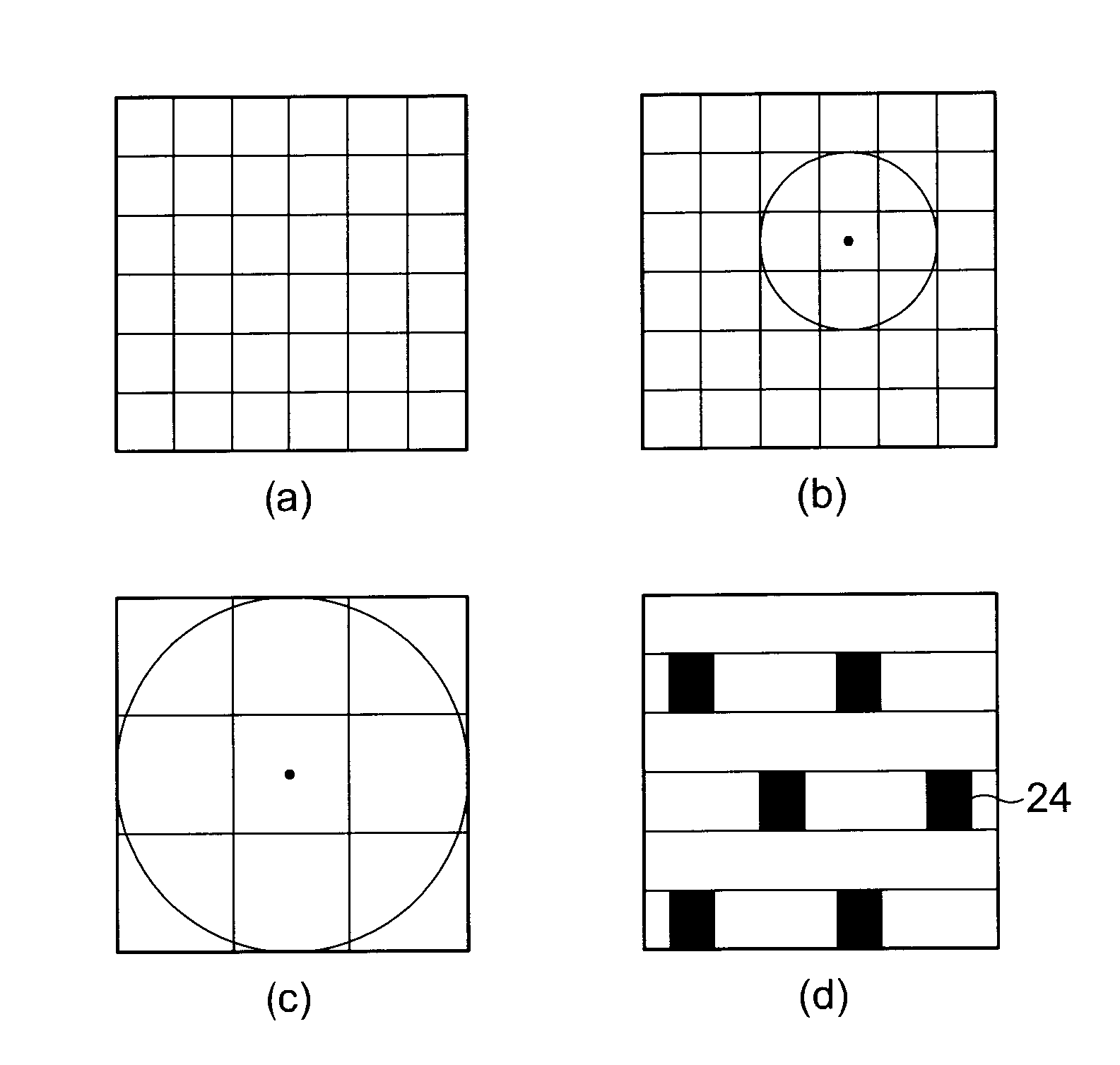
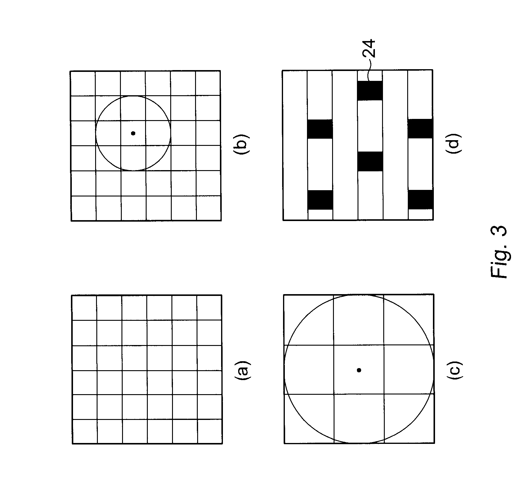
[0039]Generally, an embodiment of the invention is to strategically swap filler cells for spare cells in an IC such as a semi-custom IC. This embodiment may provide some advantages. First, strategically placing the spare cells provides more insurance that spares will be located in areas of the chip where they may be needed. Second, strategically placing the non-sequential spares, such as the combinatorial spare cells, means that these spares no longer need be tied to the locations of other spares for example, spare flip-flops. Nevertheless, the spares may still be connected in a specific pattern. Third, additional spare cells need not be added to the design, or at least not as many. That is, the spare cells need not increase the size of the chip, or at least not as mu...


PUM


Abstract

A design method for an integrated circuit adds spare cells in a System-on-Chip to allow for Engineering Change Orders (ECOs) to be performed at a later stage in the design. This method can be used to provide a second version of the chip having minimal alterations performed in a short cycle time. The spare cells can be divided into combinational and sequential cells. There is an optimum spread of combinational cells in the design for post placement repairs of the chip with just metal layer changes. The method takes into account the drive strength of the spare cells as the main factor in their placement on the chip.

Description

[0001]The present application claims the benefit of U.S. Provisional Patent Application No. 60 / 921,023 filed on Mar. 30, 2007, which is hereby incorporated by reference in its entirety for all purposes as if fully set forth herein.FIELD OF THE INVENTION[0002]The present invention relates to integrated circuit and more particularly to the use of the filler cell area in a System-on-Chip integrated circuit.BACKGROUND OF THE INVENTION[0003]There are generally three types of ICs that a circuit designer may use to implement a custom design.[0004]A field-programmable gate array (FPGA) is an integrated circuit having a number of circuit blocks that can be interconnected in any desired manner by programming interconnection switches disposed on the FPGA die. Therefore, a circuit designer may program the FPGA with firmware to implement any circuit that the FPGA is capable of implementing.[0005]A full-custom application-specific integrated circuit (ASIC) is laid out on the transistor level to i...

Claims


Application Information

Patent Timeline
Patent Type & Authority Applications(United States)
IPC IPC(8): H01L29/76G06F17/50
CPCG06F17/5072G06F30/392
Inventor TRIPATHI, ANSHUMAN
Owner STMICROELECTRONICS SRL
Why Eureka
Try Eureka