Piezoelectric oscillator

a technology of piezoelectric oscillator and oscillator, which is applied in the direction of oscillation generator, pulse technique, instruments, etc., can solve the problems of delaying oscillation start time, increasing power consumption, and degrading the negative resistance, so as to improve the negative resistance and increase the gain of the amplifier. , the effect of increasing the gain of the amplifier

Inactive Publication Date: 2008-10-02
PANASONIC CORP
View PDF6 Cites 14 Cited by
  • Summary
  • Abstract
  • Description
  • Claims
  • Application Information

AI Technical Summary

Benefits of technology

[0020]According to this arrangement, since an arbitrary bias voltage is applied to the gate of the PMOS transistor that is a constituent of the amplifier, the gate-source voltage of the PMOS transistor can be raised, and accordingly, the amplifier gain can be increased. Further, by using the NPN transistor, a greater improvement in the negative resistance can be obtained, even during a low-voltage operation.
[0

Problems solved by technology

As a result, problems such as degradation of the negative resistance and a delayed oscillation

Method used


Image

  • Piezoelectric oscillator
  • Piezoelectric oscillator
  • Piezoelectric oscillator

Examples


first embodiment

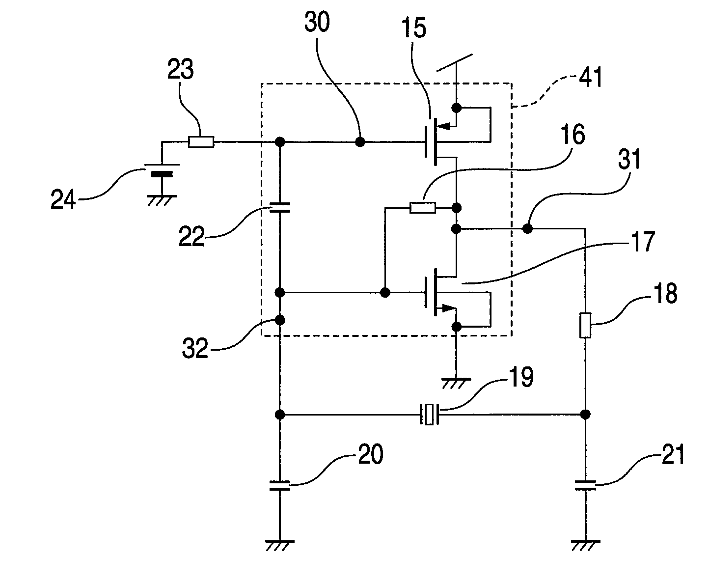
[0033]FIG. 1 is a schematic diagram showing the arrangement of a piezoelectric oscillator according to a first embodiment of the present invention. The piezoelectric oscillator of the first embodiment of the invention comprises an oscillator circuit that includes: a piezoelectric vibrator 19, such as a crystal vibrator; an NMOS transistor 17 and a PMOS transistor 15 that constitute an amplifier 41 connected in parallel to the piezoelectric vibrator 19; and load capacitors 20 and 21 that are connected in parallel to the piezoelectric vibrator 19. A gate terminal 32 of the NMOS transistor 17 and a gate terminal 30 of the PMOS transistor 15, both of which are constituents of the CMOS inverter amplifier 41, are connected by a DC cut capacitor 22, and the gate terminal 32 of the NMOS transistor 17 and an output terminal 31 of the CMOS inverter amplifier 41 are connected by a feedback resistor 16. Further, an arbitrary bias voltage 24 is to be applied to the gate terminal 30 of the PMOS t...

second embodiment

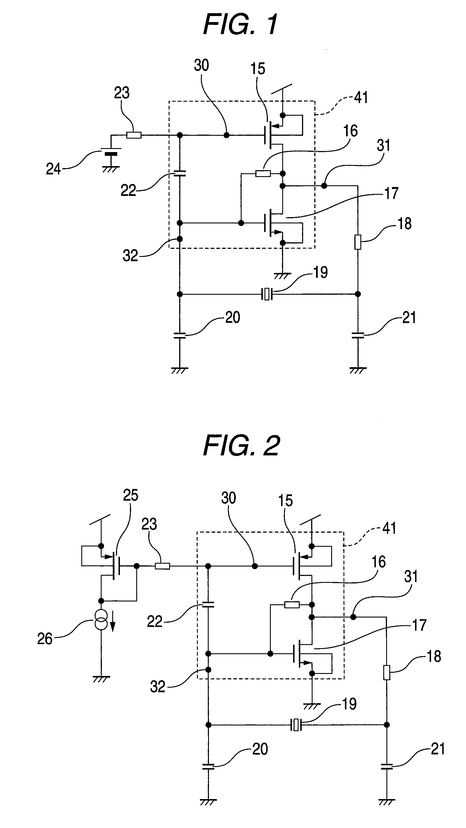
[0041]FIG. 2 is a schematic diagram showing the arrangement of a piezoelectric oscillator according to a second embodiment of the present invention. The piezoelectric oscillator of the second embodiment comprises an oscillator circuit that includes: a piezoelectric vibrator 19, such as a crystal vibrator; an NMOS transistor 17 and a first PMOS transistor 15, which constitute an amplifier 41 connected in parallel to the piezoelectric vibrator 19; and load capacitors 20 and 21, which are connected in parallel to the piezoelectric vibrator 19. A gate terminal 32 of the NMOS transistor 17 and a gate terminal 30 of the first PMOS transistor 15, which together constitute the amplifier 41, are connected by a DC cut capacitor 22, and the gate terminal 32 of the NMOS transistor 17 and an output terminal 31 of the amplifier 41 are connected by a feedback resistor 16. Further, an arbitrary bias voltage is applied to the gate terminal 30 of the first PMOS transistor 15 via a high-frequency elim...

third embodiment

[0045]FIG. 5 is a schematic diagram showing the arrangement of a piezoelectric oscillator according to a third embodiment of the present invention. According to the piezoelectric oscillator of the third embodiment, an NPN transistor 50 is used to replace the NMOS transistor 17 of the piezoelectric oscillator in FIG. 1, for the first embodiment. It should further be noted that the NPN transistor 50 may also be used to replace the NMOS transistor 17 of the piezoelectric oscillator in FIG. 2, for the second embodiment.

[0046]In the first and second embodiments, the negative resistance depends on the gain for the NMOS transistor 17, and when as shown in FIG. 5 the NPN transistor 50 is employed instead of the NMOS transistor 17, more improvement for the negative resistance can be obtained.

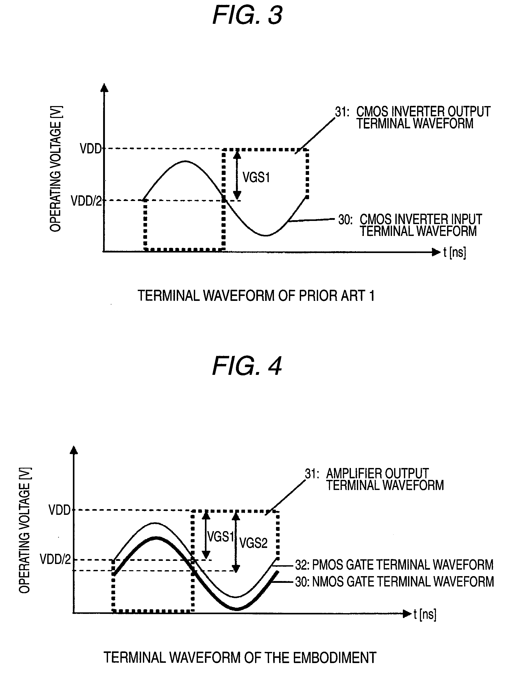
[0047]As described above, according to the piezoelectric oscillator of this embodiment, when an arbitrary bias voltage is applied to the gate of a PMOS transistor 15 of an amplifier 41, the gate-source v...


PUM


Abstract

For a piezoelectric oscillator according to the present invention, an oscillator circuit includes: a piezoelectric vibrator; an NMOS transistor and a PMOS transistor that constitute an amplifier connected in parallel to the piezoelectric vibrator; and load capacitors connected in parallel to the piezoelectric vibrator. The gate terminals of the NMOS transistor and the PMOS transistor, which are constituents of the amplifier, are connected by a DC cut capacitor, and the gate terminal of the NMOS transistor and the output terminal of the amplifier are connected by a feedback resistor. An arbitrary bias voltage, to be applied to the gate terminal of the PMOS transistor via a high-frequency elimination resistor, is generated by a circuit provided by a diode-connected, second PMOS transistor.

Description

BACKGROUND OF THE INVENTION[0001]1. Field of the Invention[0002]The present invention relates to a piezoelectric oscillator for oscillating a piezoelectric vibrator, such as a crystal vibrator.[0003]2. Description of the Related Art[0004]A temperature-compensated crystal oscillator is a crystal oscillator that is employed to provide a reference frequency for a cellular phone, and that offsets a thermal characteristic of a crystal vibrator (a piezoelectric vibrator), and possesses a property such that there is little variation in frequency due to temperature changes. Regards oscillator use, there has been a recent increased demand for temperature-compensated crystal oscillators that can be operated, at low voltages, in cellular phones and GPS systems.[0005]A conventional crystal oscillator circuit (prior art 1) is shown in FIG. 9. This crystal oscillator circuit, employed for a temperature-compensated crystal oscillator, comprises a CMOS inverter amplifier 40, which includes a PMOS t...

Claims


Application Information

Patent Timeline
IPC IPC(8): H03B5/32H03B5/36
CPCH03B5/364
Inventor OTSUKA, TAKASHITAKEUCHI, HISATO
Owner PANASONIC CORP
Why Eureka
Try Eureka