Chip scale power converter package having an inductor substrate

a power converter and inductor substrate technology, applied in the direction of magnets, magnetic bodies, semiconductor/solid-state device details, etc., can solve the problems of high component cost, large package, and disadvantages of package disadvantageous use of valuable printed circuit board space, so as to improve assembly efficiency

Active Publication Date: 2008-10-02
ALPHA & OMEGA SEMICON INC
View PDF14 Cites 41 Cited by
  • Summary
  • Abstract
  • Description
  • Claims
  • Application Information

AI Technical Summary

Benefits of technology

[0008]The chip scale power converter in accordance with the invention combines an inductor with the chip scale package to improve efficiency of assembly. An inductor substrate is provided that includes an optimized planar spiral inductor. A power IC is flipped onto the inductor substrate to form the chip scale power converter.

Problems solved by technology

Power converters implemented in this way suffer the disadvantages of having higher component cost and of requiring more printed circuit board space.
The package disadvantageously uses valuable printed circuit board space.
To achieve high inductance, a large die is required resulting in a high cost and a large package.
Furthermore, complex processing is necessary in order to fabricate the planar magnetic layers.

Method used


Image

  • Chip scale power converter package having an inductor substrate
  • Chip scale power converter package having an inductor substrate
  • Chip scale power converter package having an inductor substrate

Examples


Embodiment Construction

[0027]The present invention will now be described in detail with reference to the drawings, which are provided as illustrative examples of the invention so as to enable those skilled in the art to practice the invention. Notably, the figures and examples below are not meant to limit the scope of the present invention. Where certain elements of the present invention can be partially or fully implemented using known components, only those portions of such known components that are necessary for an understanding of the present invention will be described, and detailed descriptions of other portions of such known components will be omitted so as not to obscure the invention. Further, the present invention encompasses present and future known equivalents to the components referred to herein by way of illustration.

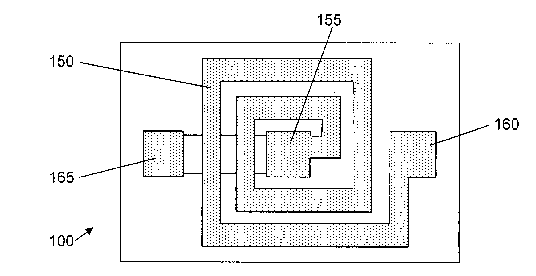
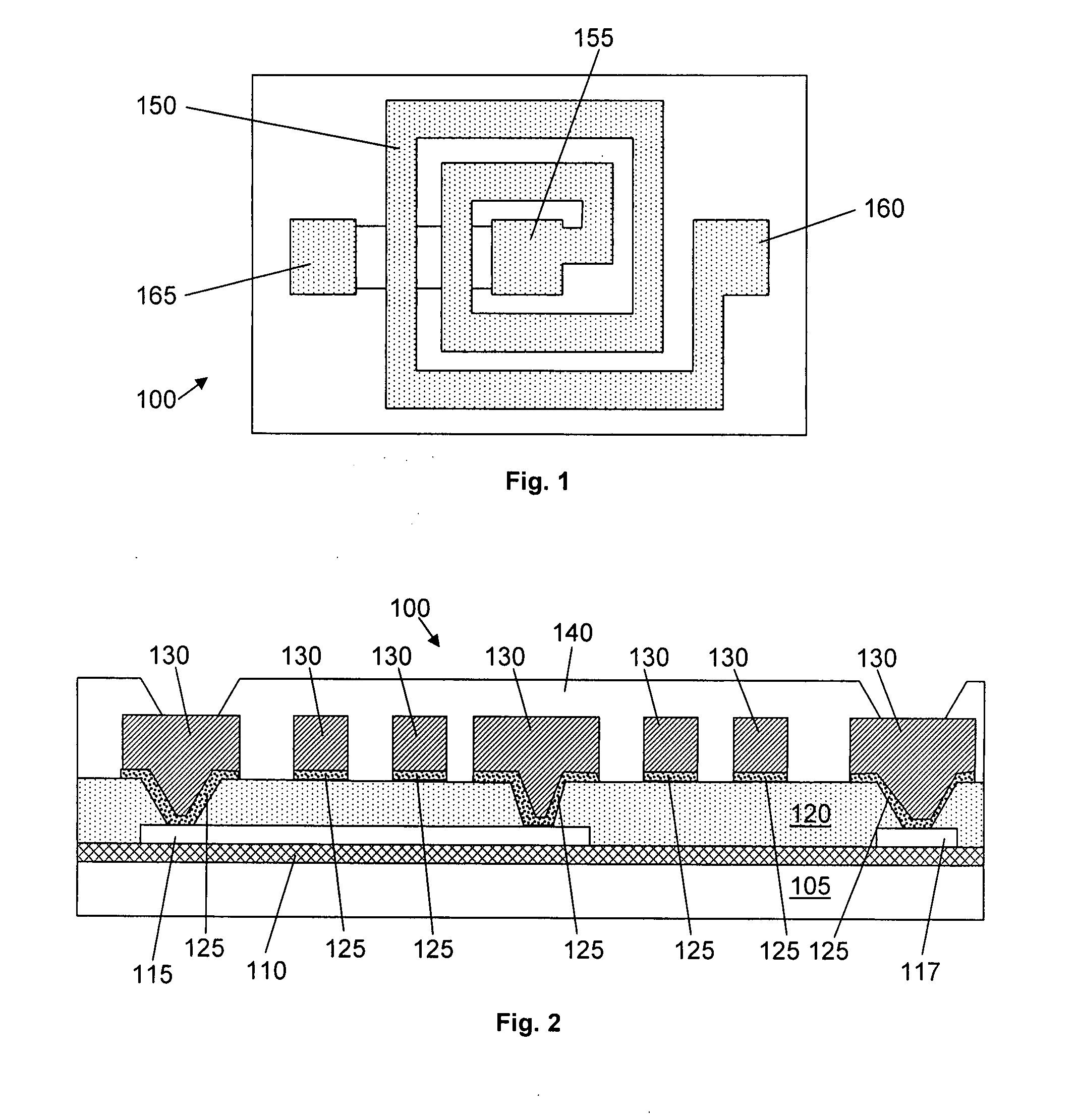
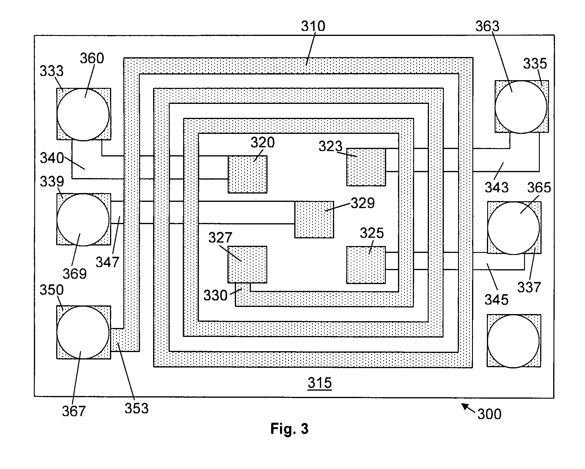
[0028]The present invention provides a chip scale power converter having an inductor substrate. An exemplary inductor substrate 100 is shown in FIG. 1 and FIG. 2. Inductor subst...


PUM

PropertyMeasurementUnit
thicknessaaaaaaaaaa
thicknessaaaaaaaaaa
magneticaaaaaaaaaa

Abstract

A chip scale power converter package having an inductor substrate and a power integrated circuit flipped onto the inductor substrate is disclosed. The inductor substrate includes a high resistivity substrate having a planar spiral inductor formed thereon.

Description

BACKGROUND OF THE INVENTION[0001]1. Field of the Invention[0002]The present invention generally relates to chip scale packaging and more particularly to a chip scale power converter package having an inductor substrate.[0003]2. Description of Related Art[0004]It is well known to include a discrete inductor on the printed circuit board when implementing a power converter circuit. For example, the Analogic™TECH 1 MHz 400 mA Step-Down Converter (AAT1143) requires the use of a discreet inductor. Power converters implemented in this way suffer the disadvantages of having higher component cost and of requiring more printed circuit board space.[0005]Discrete inductors co-packaged with power ICs and other components are also well known. For example, the LTM®4600 DC / DC power converter available from Linear Technology Corporation of Milpitas, Calif., includes a built-in inductor in a 15 mm×15 mm×2.8 mm package. The package disadvantageously uses valuable printed circuit board space.[0006]It i...

Claims


Application Information

Patent Timeline
Patent Type & Authority Applications(United States)
IPC IPC(8): H01F17/04H01F27/28
CPCH01L23/5227Y10T29/4902H01L2224/16H01L2924/0102H01L2924/01057H01L2924/01078H01L2924/01079H01L2924/04941H01L2924/1902H01L2924/3025H01L2924/01019H01L2924/13091H01L2924/1461H01L23/645Y10T29/49075H01L2924/00H01L2924/00014H01L2924/00011H01L2224/16265H01L2224/0401
Inventor HEBERT, FRANCOISSUN, MING
Owner ALPHA & OMEGA SEMICON INC
Why Eureka
Try Eureka