

Method of forming ultra thin chips of power devices
- Summary
- Abstract
- Description
- Claims
- Application Information
AI Technical Summary
Benefits of technology
Problems solved by technology
Method used
Image

Examples
first embodiment
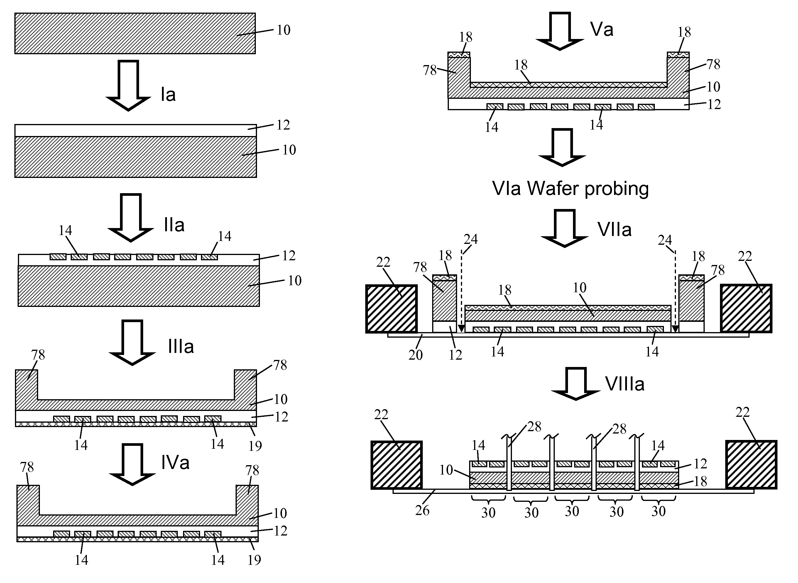
[0057]FIG. 1 illustrates the overall process flow for making complete ultra thin power device chips 30 under the present invention. In this embodiment, the starting material is a wafer of an original thickness and made of a highly doped semiconductor substrate 10. The diameter of the wafer is typically in the range of from about 6″ to about 8″ although the application of the present invention is not limited to this range. Following STEP Ia, called epi growth, an epitaxial layer 12 is grown on top of the highly doped semiconductor substrate 10. Following STEP IIa, called front-side device fabrication, a plurality of fabricated devices 14 are produced on the front-side of the wafer. It is remarked that numerous methods are known in the art for front-side device fabrication. For those skilled in the art, front-side device fabrication includes photolithographic masking, dopant diffusion, ion implantation, selective pattern etching, epitaxial layer growth, material deposition.
[0058]Next,...
second embodiment
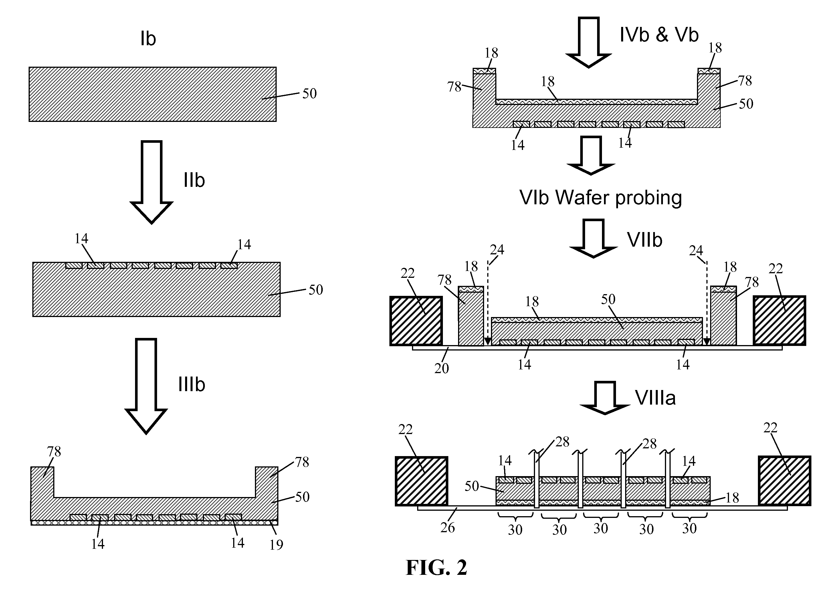
[0066]The process as illustrated in FIG. 1 is suitable for making ultra thin power semiconductor device chips with devices fabricated in epitaxial layers. FIG. 2 illustrates the overall process flow for making ultra thin power device chips 30 without an epitaxial layer under the present invention. As remarked before, device for HV application may require thick epitaxial layers that are high cost. By employing material called float zone wafer, devices for HV application can be fabricated directly on the wafer without the epitaxial layer, followed by wafer thinning to a desired thickness and back metallization. The desired thickness may be between 2 to 4 mils. In this embodiment, the starting material is, following a STEP Ib called float zone wafer fabrication, a wafer of an original thickness and made of a float zone semiconductor wafer 50 that is substantially cheaper than an equivalent epitaxial layer. An example of the float zone semiconductor wafer 50 has a lightly-doped N-type b...
PUM
 Abstract
Description
Claims
Application Information