Light emitting apparatus and method for manufacturing same

a technology manufacturing method, which is applied in the direction of lasers, semiconductor lasers, solid-state devices, etc., can solve the problems of characteristic variation and reliability degradation of light emitting apparatus, and be desirable reduced

Inactive Publication Date: 2008-10-09
KK TOSHIBA
View PDF7 Cites 22 Cited by
  • Summary
  • Abstract
  • Description
  • Claims
  • Application Information

AI Technical Summary

Problems solved by technology

Such stress may cause characteristics variation and reliability degradation of the light emitting apparatus, and hence is desirably reduced.

Method used


Image

  • Light emitting apparatus and method for manufacturing same
  • Light emitting apparatus and method for manufacturing same
  • Light emitting apparatus and method for manufacturing same

Examples


first embodiment

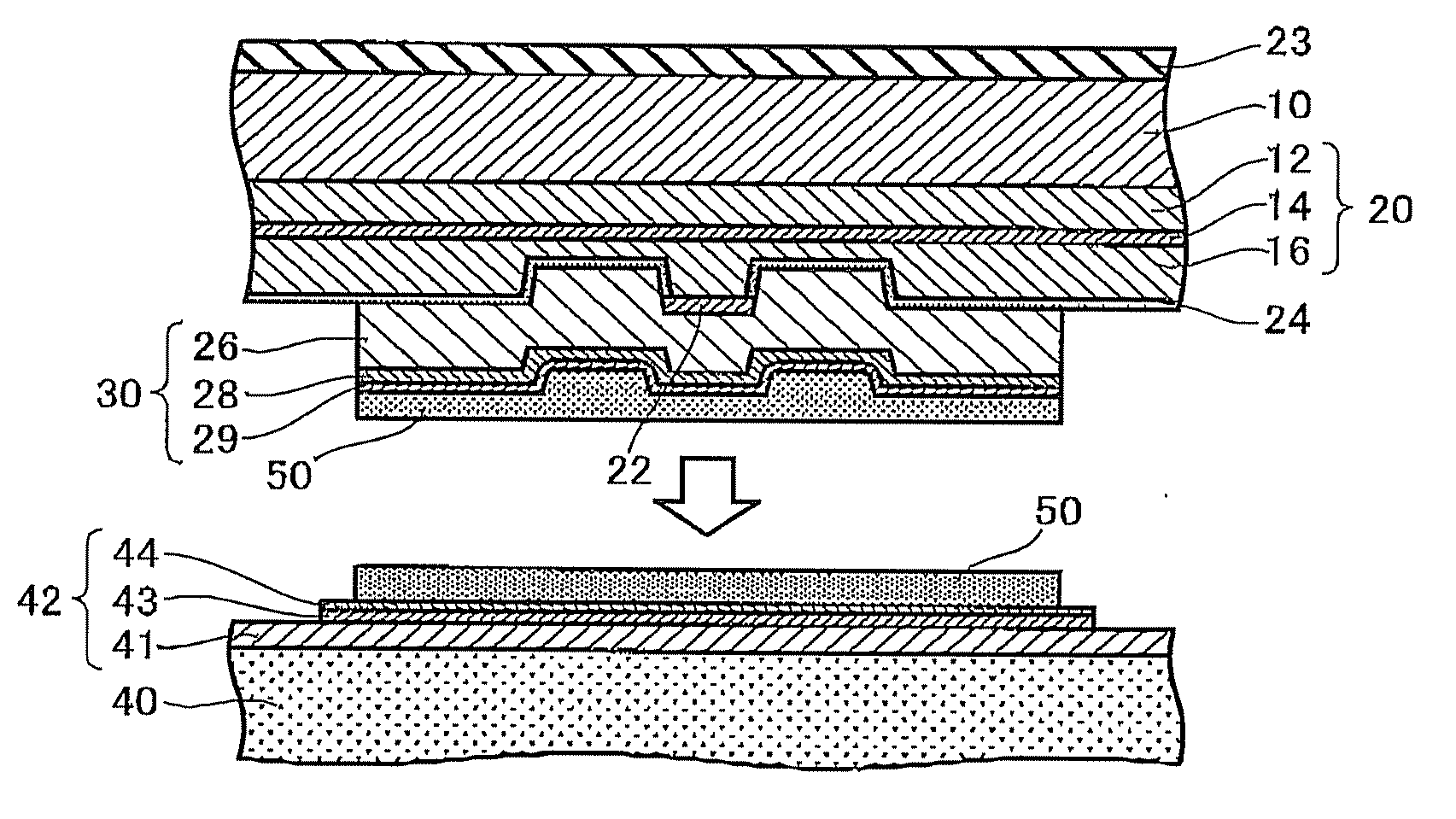
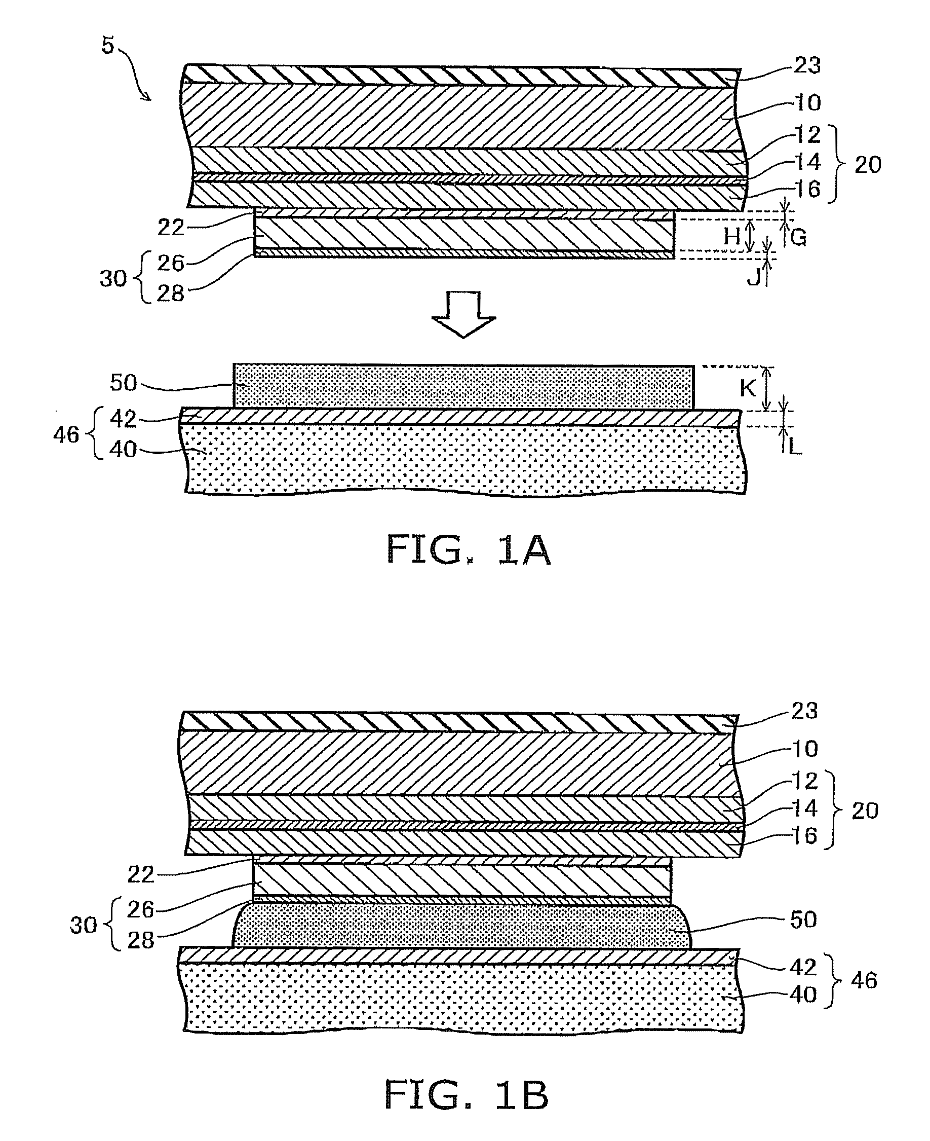
[0017]FIG. 1 shows a light emitting apparatus according to the invention. As shown in FIG. 1A, a laminated body 20 including an n-type layer 12, a light emitting layer 14, and a p-type layer 16 is formed on a semiconductor substrate 10 by MOCVD (metal organic chemical vapor deposition), for example.

[0018]Subsequently, an ohmic electrode 22 in ohmic contact with the laminated body 20 is formed on the laminated body 20. Furthermore, the ohmic electrode 22 is covered with a pad electrode 30, which includes a gold layer 26 thicker than the ohmic electrode 22 and a metal barrier layer 28 provided thereon. An n-side electrode 23 is formed on the substrate 10. Thus the light emitting element 5 is completed.

[0019]The metal constituting the ohmic electrode 22 in contact with the p-type layer 16 can be Ti (titanium) to decrease contact resistance. The ohmic electrode 22 (thickness G) is preferably composed of Ti / Pt (platinum), Ti / Pt / Au (gold), Ti / Mo (molybdenum), or Ti / Mo / Au. The thickness G ...

second embodiment

[0032]FIG. 3 is a schematic view showing a light emitting apparatus according to a While a nitride semiconductor laser apparatus is described in this embodiment, the material is not limited to nitrides, but other materials may also be used. The term “nitride semiconductor” used herein refers to a semiconductor represented by (AlxB1-x)yGazIn1-y-zN (0≦x≦1, 0≦y≦1, 0≦z≦1, y+z≦1), and also encompasses those containing As and / or P as group V elements and those containing p-type or n-type impurities.

[0033]The substrate 10 is made of n-type GaN. As shown in FIG. 3, the p-type layer 16 of the laminated body 20 made of a nitride semiconductor has a ridge waveguide 17 (width X and height M) and grooves 18 (width Y) on both sides thereof. An insulating film 24 illustratively made of SiO2 is formed outside the upper portion of the ridge waveguide 17 constituting an optical resonator A p-side electrode to serve as an ohmic electrode 22 (thickness G) is formed on top of the ridge waveguide 17. He...


PUM

PropertyMeasurementUnit
thicknessaaaaaaaaaa
thicknessaaaaaaaaaa
thicknessaaaaaaaaaa

Abstract

A light emitting apparatus includes: a light emitting element including a laminated body, an electrode provided on the laminated body, and a pad electrode provided on the electrode, the laminated body including a semiconductor light emitting layer; a mounting member having a metal bonding layer; and an alloy solder containing gold for bonding the pad electrode to the metal bonding layer. The pad electrode has at least a first gold layer provided on the electrode and being thicker than the electrode and a first metal barrier layer provided on the first gold layer, and the melting point of the alloy solder is lower than the melting point of alloys with elements constituting the first metal barrier layer and the alloy solder.

Description

CROSS-REFERENCE TO RELATED APPLICATIONS[0001]This application is based upon and claims the benefit of priority from the prior Japanese Patent Application No. 2007-100100, filed on Apr. 6, 2007; the entire contents of which are incorporated herein by reference.BACKGROUND OF THE INVENTION[0002]1. Field of the Invention[0003]This invention relates to a light emitting apparatus and a method for manufacturing the same[0004]2. Background Art[0005]The junction-down structure of a light emitting apparatus such as a semiconductor laser and an LED (light emitting diode), in which structure the light emitting layer side is located close to the heat sink, is superior in heat dissipation. In this structure, an electrode provided on the semiconductor laminated body including the light emitting layer is bonded to the metal bonding layer of the mounting member with an alloy solder, for example.[0006]A light emitting apparatus may be subjected to stress due to temperature increase and decrease durin...

Claims


Application Information

Patent Timeline
Patent Type & Authority Applications(United States)
IPC IPC(8): H01L33/00H01L33/36H01L33/62
CPCH01L33/40H01L33/62H01S5/0224H01S5/02272H01S5/22H01L2224/16H01L24/05H01L24/29H01L24/32H01L2224/04026H01L2224/05001H01L2224/05008H01L2224/05023H01L2224/05024H01L2224/05027H01L2224/05085H01L2224/05144H01L2224/05166H01L2224/05169H01L2224/05572H01L2224/05669H01L2224/05684H01S5/0234H01S5/0237H01L2924/00014H01L2924/01078H01L2924/01079H01L2924/013H01L2924/01042
Inventor HOSOKAWA, TADAAKIHORIUCHI, OSAMUMATSUYAMA, TAKAYUKIOKADA, MAKOTO
Owner KK TOSHIBA
Why Eureka
Try Eureka