
Self-Aligned Trench MOSFET and Method of Manufacture

a technology of self-alignment and trench mosfet, which is applied in the direction of basic electric elements, electrical equipment, semiconductor devices, etc., can solve the problems of source contact alignment errors in the inability to shrink the pitch below 1 micrometer (um)

Active Publication Date: 2008-10-09
VISHAY SILICONIX LLC
View PDF91 Cites 52 Cited by
  • Summary
  • Abstract
  • Description
  • Claims
  • Application Information

AI Technical Summary

Benefits of technology

The present technology provides an improved trench MOSFET with improved performance. The MOSFET includes a drain region, a plurality of gate regions, a plurality of gate insulator regions, a field insulator region, a plurality of source regions, and a plurality of source / body contact spacers. The MOSFET also includes a method of fabricating the MOSFET that includes depositing layers, etching trenches, and depositing dielectric layers. The technical effects of the present technology include improved performance and reliability of the trench MOSFET.

Problems solved by technology

However, the ability to shrink the pitch below 1 micrometer (um) has been limited by source contact alignment errors, even when deep-ultraviolet (DUV) photolithography is used.

Method used


Image

  • Self-Aligned Trench MOSFET and Method of Manufacture
  • Self-Aligned Trench MOSFET and Method of Manufacture
  • Self-Aligned Trench MOSFET and Method of Manufacture

Examples


Embodiment Construction

[0009]Reference will now be made in detail to the embodiments of the present technology, examples of which are illustrated in the accompanying drawings. While the present technology will be described in conjunction with these embodiments, it will be understood that they are not intended to limit the invention to these embodiments. On the contrary, the invention is intended to cover alternatives, modifications and equivalents, which may be included within the scope of the invention as defined by the appended claims. Furthermore, in the following detailed description of the present technology, numerous specific details are set forth in order to provide a thorough understanding of the present technology. However, it is understood that the present technology may be practiced without these specific details. In other instances, well-known methods, procedures, components, and circuits have not been described in detail as not to unnecessarily obscure aspects of the present technology.

[0010]...


PUM


Abstract

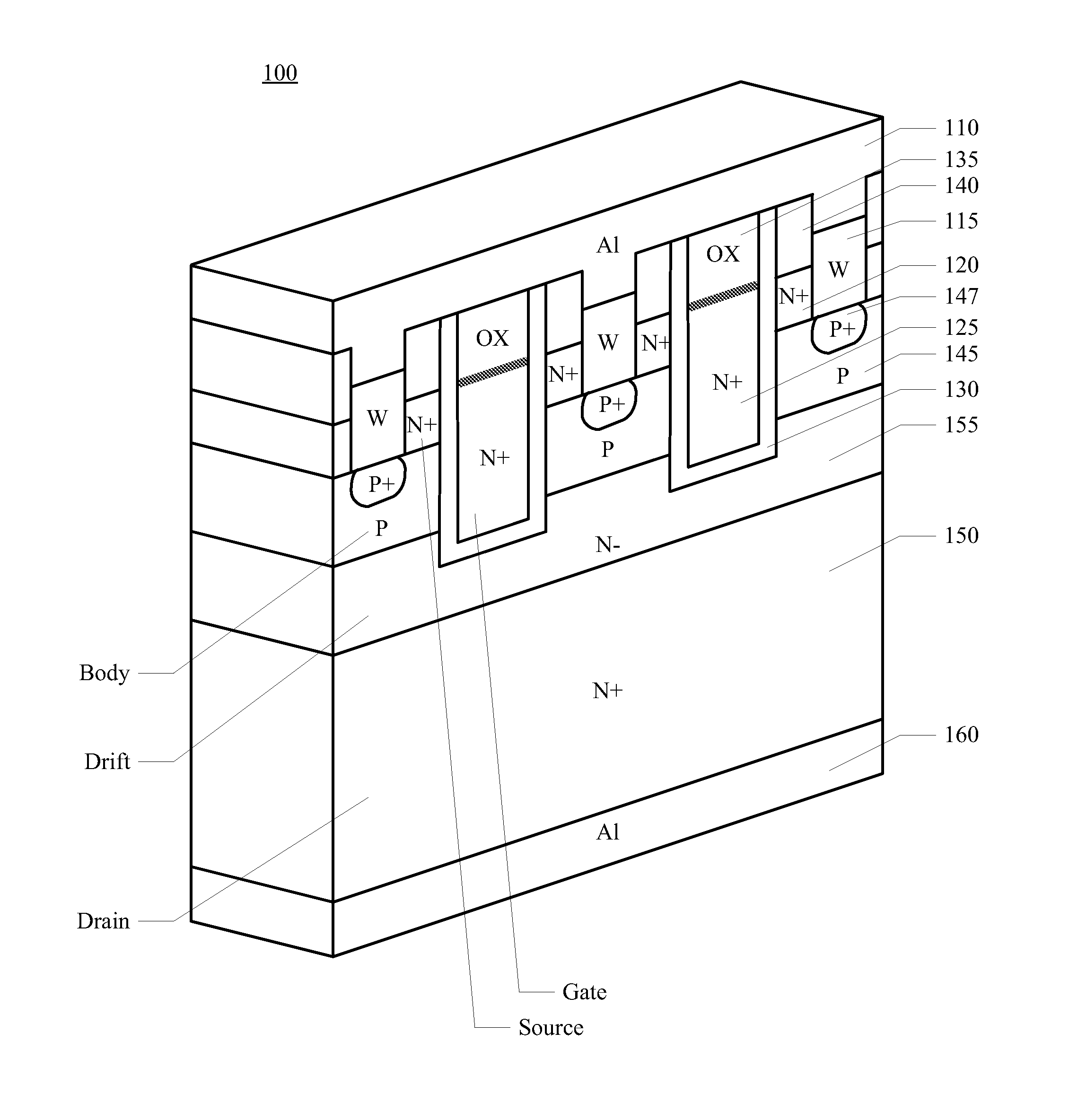
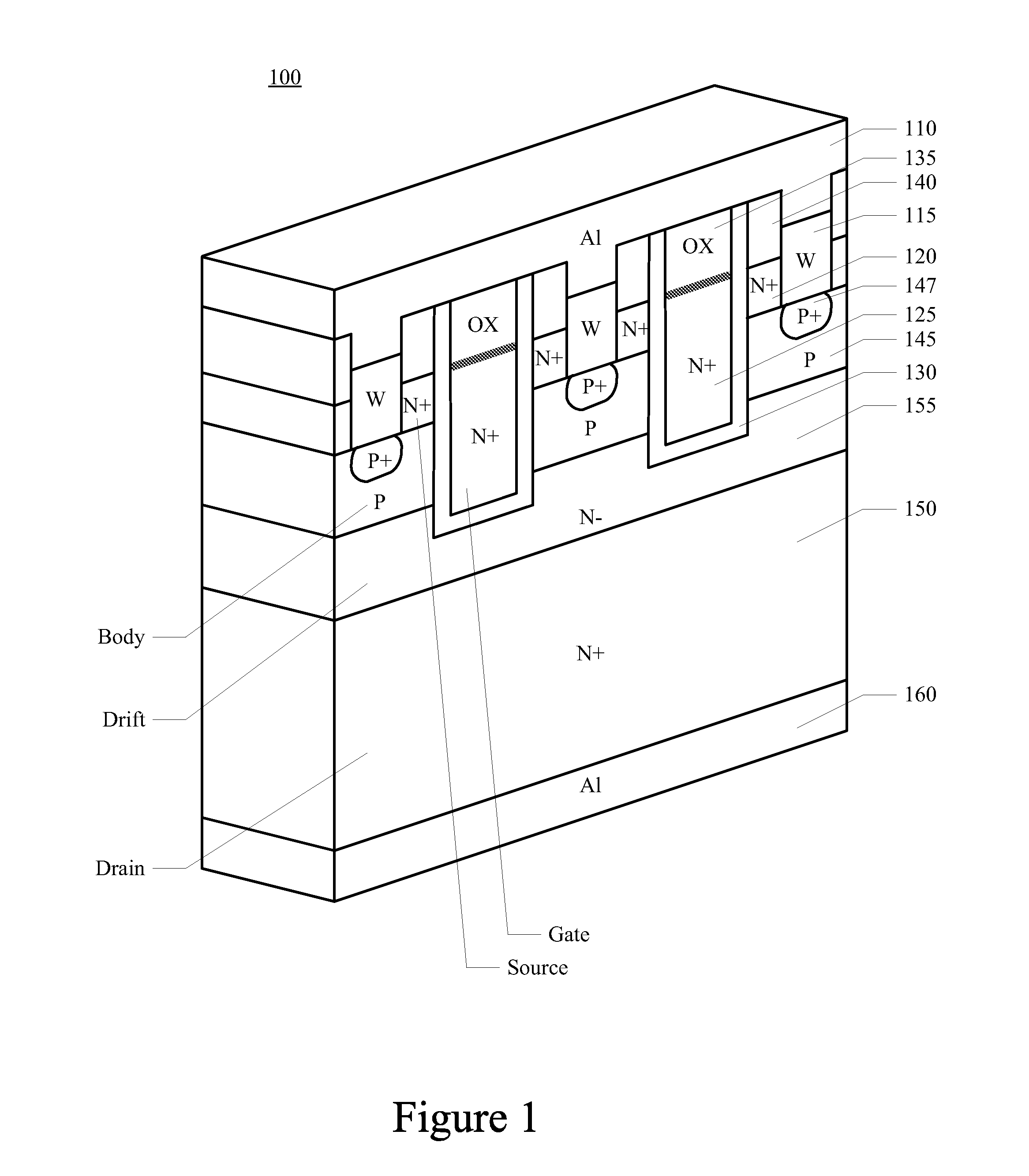
A trench metal-oxide-semiconductor field effect transistor (MOSFET), in accordance with one embodiment, includes a drain region, a plurality of gate regions disposed above the drain region, a plurality of gate insulator regions each disposed about a periphery of a respective one of the plurality of gate regions, a plurality of source regions disposed in recessed mesas between the plurality of gate insulator regions, a plurality of body regions disposed in recessed mesas between the plurality of gate insulator regions and between the plurality of source regions and the drain region. The MOSFET also includes a plurality of body contact regions disposed in the each body region adjacent the plurality of source regions, a plurality of source / body contact spacers disposed between the plurality of gate insulator regions above the recessed mesas, a source / body contact disposed above the source / body contact spacers, and a plurality of source / body contact plugs disposed between the source / body contact spacers and coupling the source / body contact to the plurality of body contact regions and the plurality of source regions.

Description

CROSS-REFERENCE TO RELATED APPLICATIONS[0001]This application claims the benefit of U.S. Provisional Application No. 60 / 921,792 filed Apr. 3, 2007.BACKGROUND OF THE INVENTION[0002]To reduce the drain-to-source on-resistance (Rdson) in power metal-oxide-semiconductor field effect transistors (MOSFET), numerous novel structures have been proposed and implemented. In trench based MOSFETs, shrinking the lateral pitch to increase cell density has been used to effectively reduce Rdson of the multi-cell MOSFETs. However, the ability to shrink the pitch below 1 micrometer (um) has been limited by source contact alignment errors, even when deep-ultraviolet (DUV) photolithography is used. Accordingly, there is a continued need to further reduce the Rdson of MOSFETs and improved techniques for fabricating such MOSFETs.SUMMARY OF THE INVENTION[0003]Embodiments of the present technology provide an improved trench metal-oxide-semiconductor field effect transistor (MOSFET). More specifically, embo...

Claims


Application Information

Patent Timeline
Patent Type & Authority Applications(United States)
IPC IPC(8): H01L29/78H01L21/336
CPCH01L29/1095H01L29/41766H01L29/456H01L29/4925H01L29/7813H01L29/66719H01L29/66727H01L29/66734H01L29/4933
Inventor LI, JIANCHEN, KUO-INTERRIL, KYLE
Owner VISHAY SILICONIX LLC
Learn More