Polishing condition control apparatus and polishing condition control method of CMP apparatus

a technology of condition control apparatus and polishing condition control method, which is applied in the direction of lapping machines, manufacturing tools, instruments, etc., can solve the problems of difficult to obtain a stable, difficult to perform a highly precise polishing process, and severe polishing precision requirements, so as to prevent the wafer from being polished and processed, improve the polishing precision of the wafer, and eliminate the uneven thickness of the film thickness

Inactive Publication Date: 2008-10-09
TOKYO SEIMITSU
View PDF3 Cites 15 Cited by
  • Summary
  • Abstract
  • Description
  • Claims
  • Application Information

AI Technical Summary

Benefits of technology

[0034]According to the third aspect of the present invention, since the polishing conditions that reflect the data of the past polishing history and / or the polishing model peculiar to the apparatus can be prepared, in addition to the effect of the first or second aspect, it is possible to improve the polishing precision of the wafers.
[0035]According to the fourth aspect of the present invention, since the polishing time of the wafer is forecasted on the basis of the data of the past polishing history and / or the data of the polishing model peculiar to the apparatus, in addition to the effect of the first aspect, it is possible to forecast the polishing time more precisely.
[0036]According to the fifth aspect of the present invention, since the difference between the above measured value of the polishing time and the forecasted value thereof, and the polishing states of the wafers and the like can be monitored in real time, in addition to the effect of the first aspect, it is possible to check the polishing states of the wafers according to the specifications of the wafers and the polishing environment at any time.
[0037]According to the sixth aspect of the present invention, when the polishing state gets erroneous, the effect to that is automatically notified, and at an emergency, the polishing process is stopped immediately, and accordingly, in addition to the effect of the first or fifth aspect, it is possible to prevent the wafer from being polished and processes in an erroneous state.
[0038]According to the seventh aspect of the present invention, since the optimal polishing conditions for each polishing step of the above wafer, each polishing shaft, and / or each platen can be set in common, and accordingly, in addition to the effect of the first aspect, it is possible to eliminate the unevenness of the film thickness of wafers among the individual polishing steps, the polishing shafts and / or the platens.
[0039]According to the eighth aspect of the present invention, when the wafers are polished, the polishing conditions such as the polishing speed, the polishing pressure, the flow quantity of abrasives can be corrected / changed optimally, and accordingly, it is possible to improve the polishing precision of the film thickness of the wafers, and the unevenness of the film thickness of the wafers can be eliminated, and further increase of the polishing efficiency, and reduction of the running costs (the wastes of abrasives and the like) are achieved. Furthermore, excessive polishing and insufficient polishing are eliminated, and the occurrence of defective products can be reduced in comparison with the prior art, and accordingly, it is possible to enhance the production yield.

Problems solved by technology

In recent years, the design rules of semiconductor technologies have become toward ultrafine configurations and multilayer wiring, and the diameter of wafers has become larger, and consequently in the CMP process, requirements for polishing precision and polishing speed have become severer.
In the conventional CMP apparatus, in the case where the film thickness of the wafer is measured by the vertical direction displacement of the polishing pad, it is difficult to obtain a stable result of the film thickness measurement, and consequently, it is not possible to perform a highly precise polishing process.
Further, in the case where the CMP process is performed by the simple feedback control of the film thickness measurement, it is not possible to obtain a highly precise film thickness measurement, and consequently, the method does not cope with ultrafine and highly integrated wafers sufficiently.
On the other hand, in the case where the state of the wafer polishing is monitored by a monitor, and the polishing state of the wafers to be polished afterward is forecasted and polishing is performed, the polishing process conditions differ with the respective modules of the apparatus, that is, respective rotating axes of the polishing head (hereinafter referred to as polishing axes), and respective platens, and as a result, the film thickness of wafers after the polishing process is apt to be uneven among the modules.
As mentioned above, according to the prior art, unevenness in the film thickness of the wafers occurs among the modules.
In addition, excessive polishing and insufficient polishing easily take place, and polishing efficiency of the wafer declines, and defects occur in wafers after the polishing, and the production yield decreases.
Furthermore, expendable supplies such as abrasives are wasted more than necessary, and accordingly the running cost of the expendable supplies increases, and these have been problems in the prior art.

Method used


Image

  • Polishing condition control apparatus and polishing condition control method of CMP apparatus
  • Polishing condition control apparatus and polishing condition control method of CMP apparatus
  • Polishing condition control apparatus and polishing condition control method of CMP apparatus

Examples


Embodiment Construction

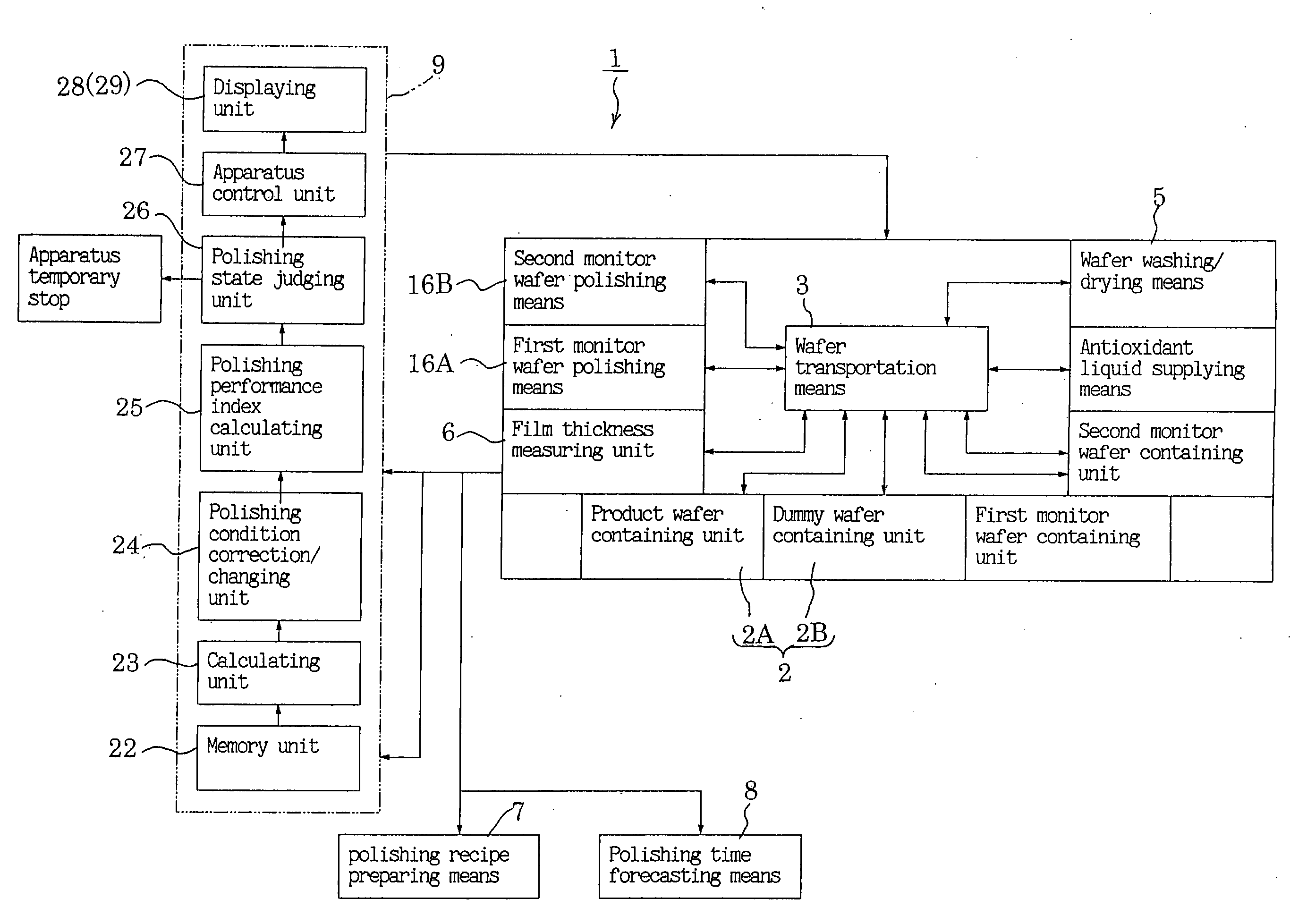
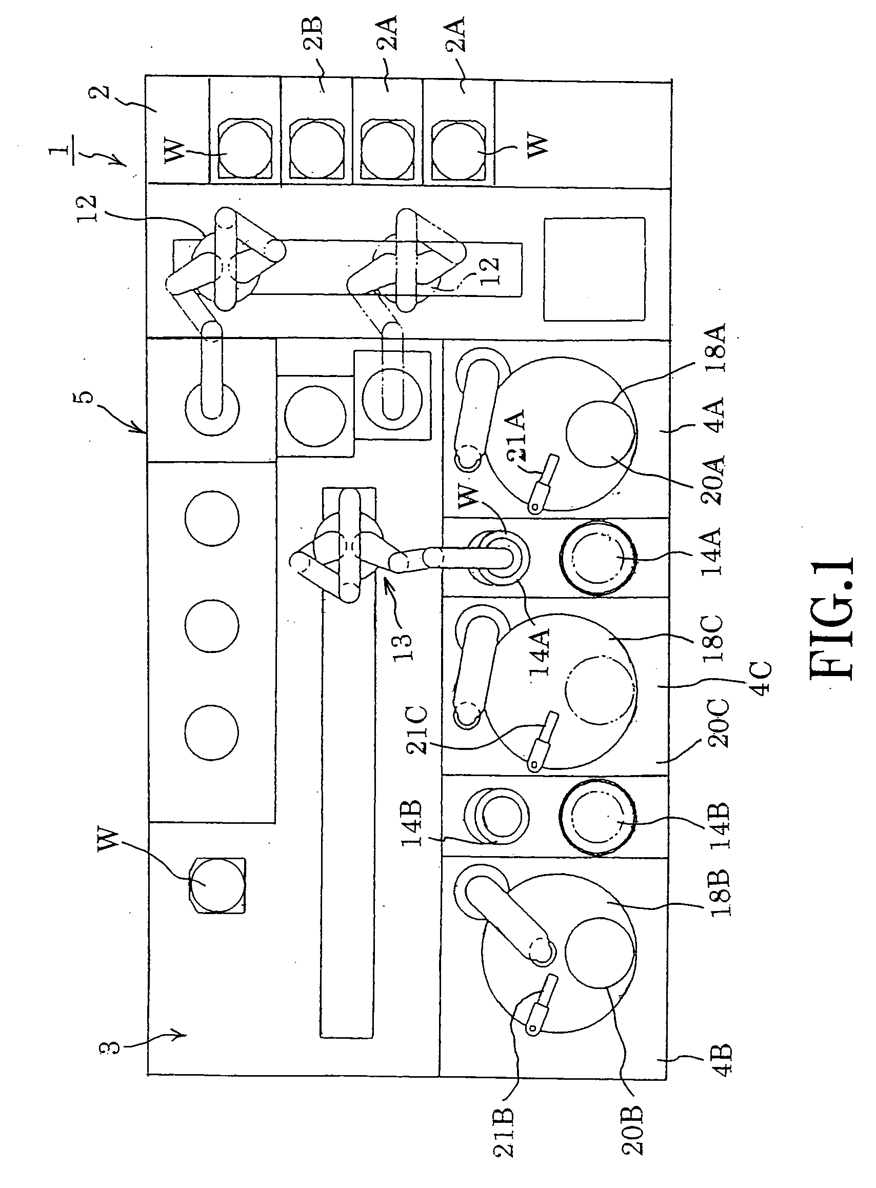
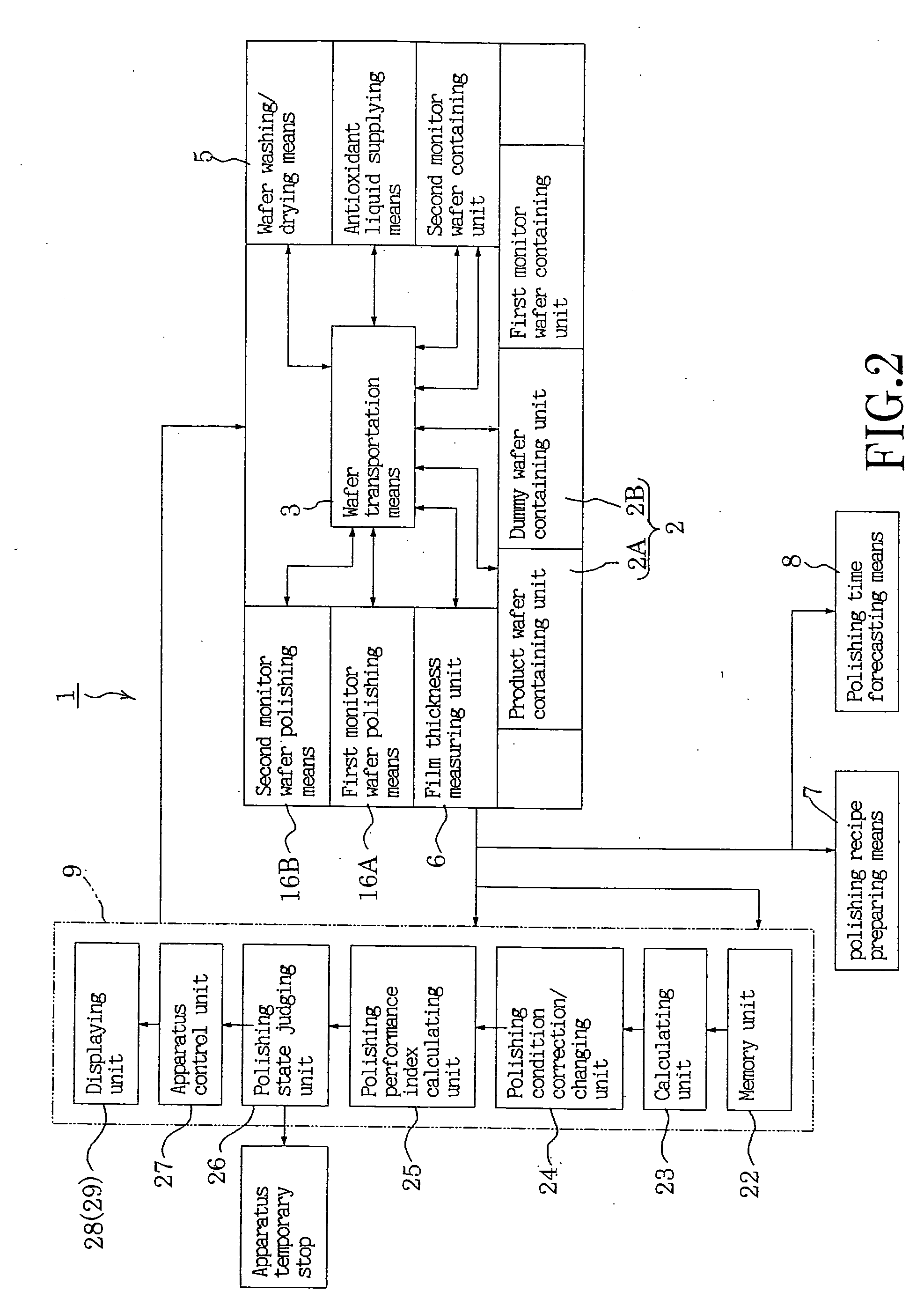
[0046]In order to achieve the object to eliminate the unevenness of the film thickness of the wafers, and, increase the polishing efficiency, reduce the running cost and enhance the production yield, the present invention is embodied by that in a CMP apparatus that polishes a film to be polished formed on the surface of a wafer, a film thickness monitoring means that measures the film thickness of the above wafer before polishing, a polishing recipe preparing means to make polishing conditions so that the polishing conditions such as polishing speed, polishing pressure, and an abrasive and the like for the wafer become optimal, a polishing time forecasting means that forecasts the polishing time of the wafer to be polished under the polishing conditions on the basis of the above measured value of the film thickness, a polishing time measuring means that measures the polishing time of the wafer polished under the above polishing conditions, and a computer that controls the measuremen...


PUM


Abstract

To eliminate the unevenness of the film thickness of the wafers, and increase the polishing efficiency, reduce the running cost and enhance the production yield. A CMP apparatus 1 includes a film thickness measuring means 6 that measures the film thickness of the wafers before polishing, a polishing recipe preparing means 7 that prepares polishing conditions so that the polishing conditions such as polishing speed, polishing pressure, and the like for the wafers become optimal, a polishing time forecasting means that forecasts the polishing time of the wafer on the basis of the optimal polishing condition and the measured value, a polishing time measuring means that measures the actual polishing time of the wafer, and a computer 9 that controls the polishing condition on the basis of the measured value and the like of the polishing time. Further, the computer 9 includes a calculating unit 23 that calculate the difference between the measured value of the polishing time and the forecasted value thereof, and a polishing condition correcting/changing unit 24 that corrects/changes the polishing conditions so that the calculated difference becomes minimal, and thereby, the correction/change of the polishing conditions is carried out in real time.

Description

BACKGROUND OF THE INVENTION[0001]1. Field of the Invention[0002]The present invention relates to a polishing condition control apparatus and a polishing condition control method of a CMP apparatus, and particularly, it relates to a polishing condition control apparatus and a polishing condition control method of a CMP apparatus for optimizing the polishing condition of a wafer.[0003]2. Description of the Related Art[0004]In recent years, the design rules of semiconductor technologies have become toward ultrafine configurations and multilayer wiring, and the diameter of wafers has become larger, and consequently in the CMP process, requirements for polishing precision and polishing speed have become severer. In addition, for example, in the wafer of the Cu damascene structure, a Cu film which is a wiring film is formed on the wafer surface, and a barrier film such as a Ta film or a Ti film or the like is formed under the Cu film, and further, an oxide film and a low dielectric consta...

Claims


Application Information

Patent Timeline
Patent Type & Authority Applications(United States)
IPC IPC(8): B24B49/03B24B51/00G06F19/00B24B37/00H01L21/304
CPCB24B49/03B24B51/00
Inventor YOKOYAMA, TOSHIYUKIFUJITA, TAKASHITANAKA, KATSUNORI
Owner TOKYO SEIMITSU
Why Eureka
Try Eureka