Semiconductor device including wiring substrate having element mounting surface coated by resin layer

a technology of semiconductor devices and wiring substrates, applied in semiconductor devices, semiconductor/solid-state device details, electrical devices, etc., can solve the problems of large component attachment height, difficult to apply such a method of thickening substrates to the field, and hinder the realization of thin structures, etc., to achieve suppressed lowering of semiconductor manufacturing yield and thin structure of semiconductor devices

Inactive Publication Date: 2008-10-16
NEC ELECTRONICS CORP
View PDF5 Cites 66 Cited by
  • Summary
  • Abstract
  • Description
  • Claims
  • Application Information

AI Technical Summary

Benefits of technology

[0041]As explained above, in accordance with the present invention, thin structure of semicondu

Problems solved by technology

When warp of such convex part is great, this constitutes obstacle in connecting the semiconductor package part shown in FIG. 15(A) to the package substrate 201.
However, employment of the method of thickening the package substrate 201 as countermeasure for warp is disadvantageous to realization of thin structure of the entirety of the semiconductor device.
For this reason, it was difficult to apply such a method of thickening the substrate to the field for which realization of thin structure of the substrate itself is required.
Moreover, in the case where package is stacked, components attachment height becomes large.
This constitutes obstacle to realization of thin structure.
Accordingly,

Method used


Image

  • Semiconductor device including wiring substrate having element mounting surface coated by resin layer
  • Semiconductor device including wiring substrate having element mounting surface coated by resin layer
  • Semiconductor device including wiring substrate having element mounting surface coated by resin layer

Examples


first embodiment

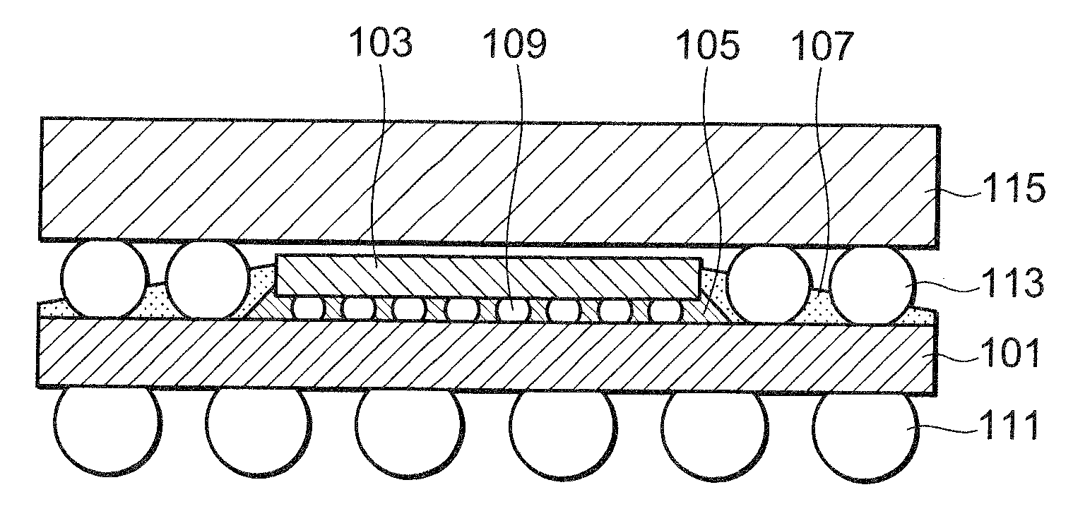
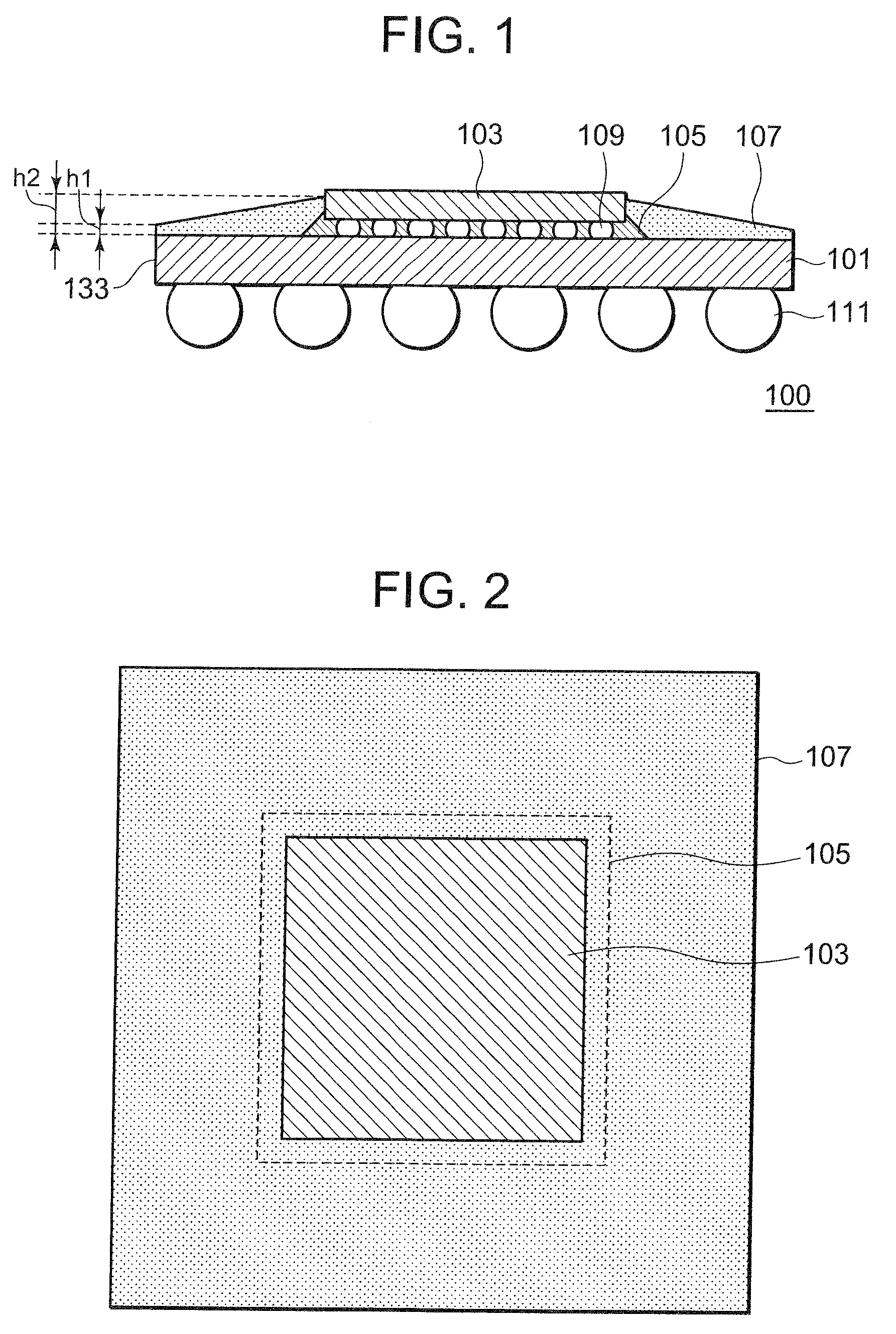
[0058]FIG. 1 is a cross sectional view showing the configuration of a semiconductor device of this embodiment. Moreover, FIG. 2 is a plan view showing the configuration of semiconductor device 100 shown in FIG. 1. In FIG. 2, bump electrode 109 and external connection electrode 111 are not shown.

[0059]The semiconductor device 100 shown in FIGS. 1 and 2 includes a first wiring substrate (package substrate 101), a first semiconductor element (first semiconductor chip 103) connected, through flip-chip bonding, to an element (chip) mounting surface of the package substrate 101, and a resin layer (underfill resin 105, outer peripheral layer 107) for coating substantially the entire chip mounting surface of the package substrate 101 including the area where the first semiconductor chip 103 is mounted.

[0060]The package substrate 101 is a wiring substrate on which a predetermined wiring structure and electrodes are provided.

[0061]Since material of the package substrate 101 is resin such as o...

second embodiment

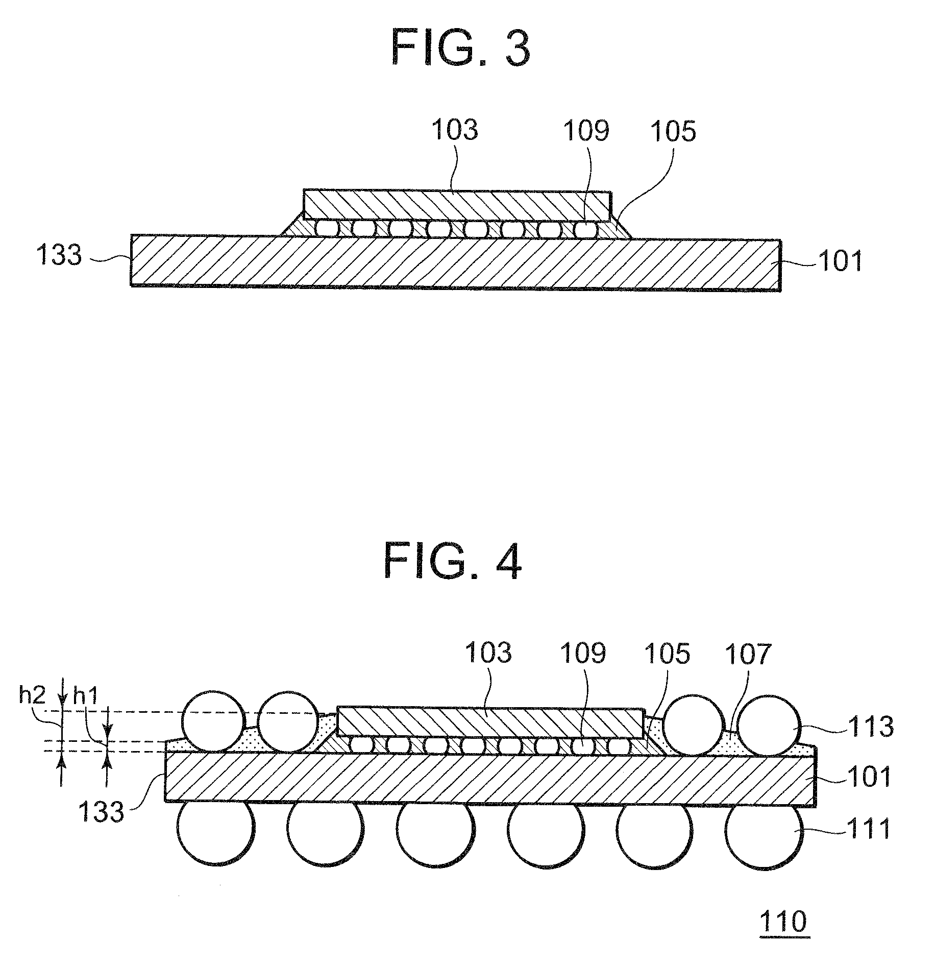
[0117]FIG. 4 is a cross sectional view showing the configuration of a semiconductor device of the second embodiment. Moreover, FIG. 5 is a plan view showing the configuration of a semiconductor device 110 shown in FIG. 4. In FIG. 5, bump electrode 109 and external connection electrode 111 are not shown.

[0118]The semiconductor device 110 shown in FIGS. 4 and 5 is similar to the semiconductor device 100 shown in FIG. 1 in the fundamental configuration, but differs from the latter in that plural bump electrodes for package connection (substrate connecting electrodes 113) are embedded within the outer peripheral layer 107.

[0119]Moreover, also in the case of the second embodiment and the embodiments succeeding thereto, it is a matter of course that the first semiconductor chip 103 may be mounted on package substrate through interposer, etc. similarly to the first embodiment. However, since explanation becomes complicated, the case including no interposer, etc. is illustrated.

[0120]The su...

third embodiment

[0143]While there is illustrated, in the second embodiment, the configuration in which semiconductor package 115 or semiconductor chip, i.e., semiconductor element is mounted on substrate connection electrode 113 (FIG. 7), any other wiring substrate may be mounted on the substrate connection electrode 113. In this embodiment, an example of such a configuration is shown.

[0144]FIG. 9 is a cross sectional view showing the configuration of a semiconductor device of this embodiment.

[0145]The semiconductor device shown in FIG. 9 is similar to the semiconductor device shown in FIG. 7 in the fundamental configuration, but differs from the latter in that second wiring substrate (interposer 117) is provided on substrate connection electrode 113.

[0146]The interposer 117 used as the second wiring substrate is provided such that the interposer 117 faces the chip mounting surface of the package substrate 101. The interposer 117 is a connection substrate for electrically connecting package substra...


PUM


Abstract

In one embodiment of the present invention, there is provided a semiconductor device including a first semiconductor element mounted, through flip-chip bonding, on the element mounting surface of a first wiring substrate, and a resin layer that coats substantially the entire element mounting surface of the first wiring substrate. The first semiconductor element has two opposite surfaces. One surface faces the element mounting surface of the first wiring substrate, and the other surface is not coated by the resin layer.

Description

BACKGROUND OF THE INVENTION[0001]1. Field of the Invention[0002]The present invention relates to a semiconductor device, and more particularly to a semiconductor device constituting a thin type semiconductor package, a package-on-package structure, and a package-on-chip structure where a semiconductor package and a semiconductor chip are stacked.[0003]2. Description of the Related Art[0004]As prior arts relating to the flip-chip type semiconductor device, there are semiconductor devices described in Japanese Patent Laid-Open Nos. 2006-108460, 2000-299414, 2000-260820, 5-283455, 2004-260138 and “High Speed Characteristic Such That Instantaneous Chance Is Not Escaped” [online] [Retrieve Jul. 18, 2006] Internet <URL: http: / / www.canon-sales.co.jp / camera / ixyd / 60 / feature04.html>.[0005]In Japanese Patent Laid-Open No. 2006-108460, it is described that, in sealing the part between a semiconductor chip and a wiring substrate by underfill resin, stress takes place resulting from thermal...

Claims


Application Information

Patent Timeline
IPC IPC(8): H01L23/48
CPCH01L21/563H01L23/3128H01L23/3157H01L24/81H01L24/83H01L24/97H01L25/105H01L2224/13144H01L2224/16225H01L2224/32225H01L2224/48227H01L2224/73203H01L2224/73265H01L2224/81205H01L2224/81801H01L2224/83102H01L2224/83851H01L2224/83862H01L2224/83951H01L2224/92125H01L2224/97H01L2924/01005H01L2924/01027H01L2924/01029H01L2924/01078H01L2924/01079H01L2924/01082H01L2924/12044H01L2924/15311H01L2924/15331H01L2924/18161H01L2924/19041H01L2924/19043H01L2924/19105H01L2924/19106H01L2224/81H01L24/32H01L24/48H01L2924/01006H01L2924/01033H01L2924/01076H01L2224/73204H01L2224/16145H01L2224/32145H01L2924/3511H01L2924/00012H01L2924/00H01L2225/1023H01L2225/1058H01L2924/3512H01L2924/00015H01L2924/12041H01L2224/2919H01L2224/73253H01L2924/00014H01L2924/181H01L2924/00011H01L2924/0665H01L2224/0401H01L2224/45099H01L2224/45015H01L2924/207
Inventor INOMATA, TERUJI
Owner NEC ELECTRONICS CORP
Why Eureka
Try Eureka