Semiconductor device

a technology of semiconductor chips and semiconductor chips, applied in semiconductor devices, semiconductor/solid-state device details, electrical apparatus, etc., can solve the problem that the binder which overflowed from the semiconductor chip of the second stage will cover the surface electrode of the semiconductor chip of the first stage, and achieve the effect of reducing preventing the generation of wire peeling, and suppressing the wire bonding property

Inactive Publication Date: 2008-10-16
RENESAS TECH CORP
View PDF3 Cites 2 Cited by
  • Summary
  • Abstract
  • Description
  • Claims
  • Application Information

AI Technical Summary

Benefits of technology

[0027]Since the filmy adhesive adhered to the back surface of the semiconductor chip of the highest stage is the thinnest among the filmy adhesives of the back surface of each of a plurality of semiconductor chips, the influence to the ultrasonic wave and load of wire bonding by softening of the fi...

Problems solved by technology

Therefore, when using a paste state binder as a die bonding material, the inconvenience that the binder which overflowed fro...

Method used


Image

  • Semiconductor device
  • Semiconductor device
  • Semiconductor device

Examples


embodiment 1

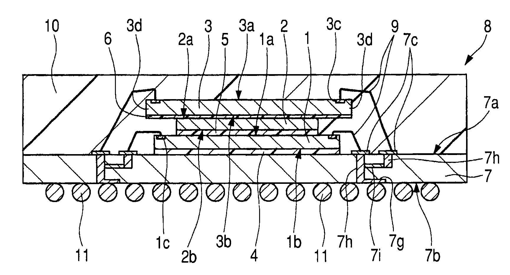
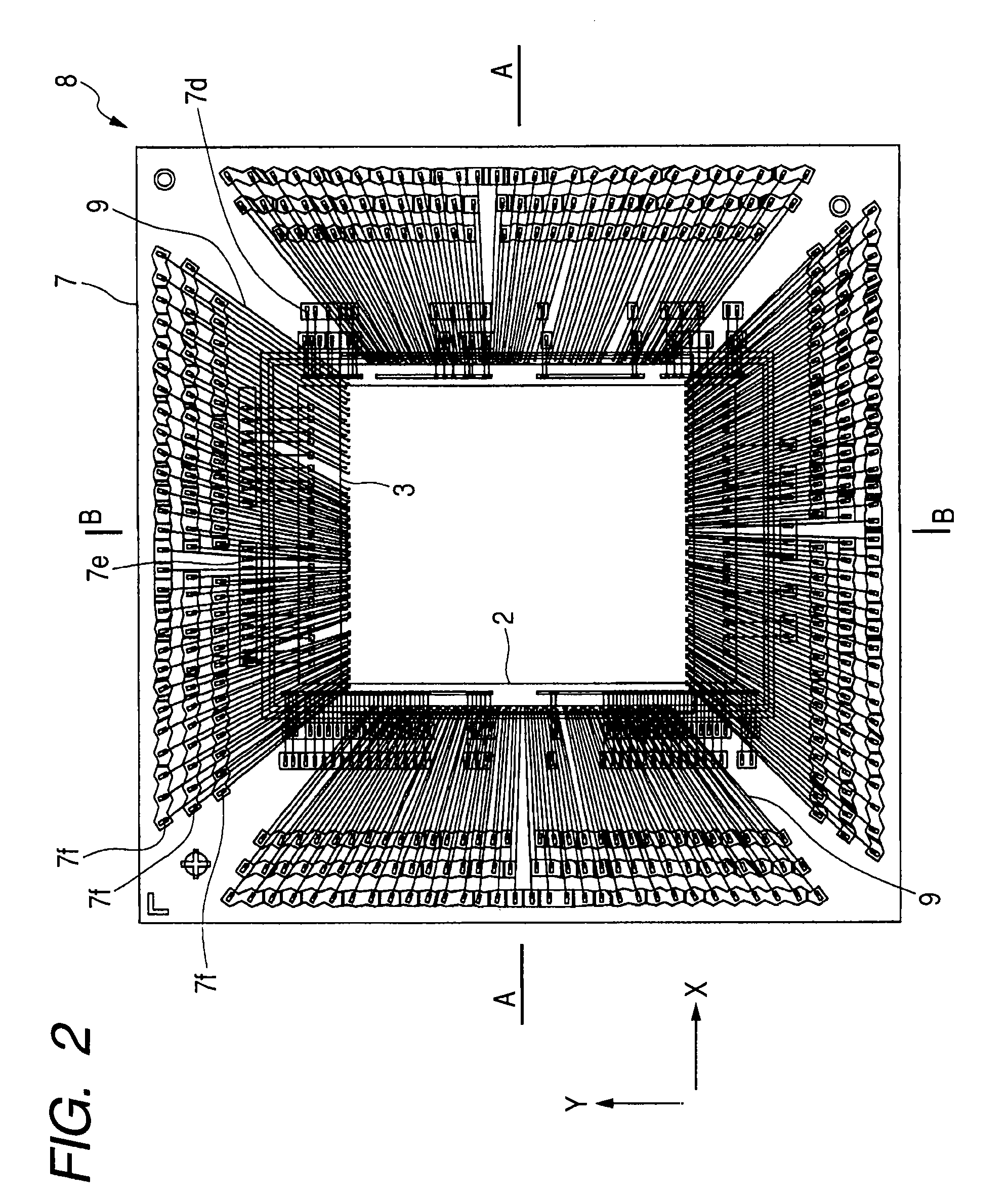
[0061]FIG. 1 is a cross-sectional view showing an example of the structure of the semiconductor device of Embodiment 1 of the present invention, FIG. 2 is a plan view penetrating a sealing body and showing an example of the fine structure of the semiconductor device shown in FIG. 1, FIG. 3 is a cross-sectional view showing an example of the structure cut along the A-A line of FIG. 2, FIG. 4 is a partially expanded cross-sectional view expanding and showing an example of the structure of the section C shown in FIG. 3, FIG. 5 is a cross-sectional view showing an example of the structure cut along the B-B line of FIG. 2, and FIG. 6 is a partially expanded cross-sectional view expanding and showing an example of the structure of the section D shown in FIG. 5. And, FIG. 7 is a plan view penetrating a sealing body and showing an example of a wiring state of the first stage chip in the semiconductor device shown in FIG. 2, FIG. 8 is a cross-sectional view showing an example of the structur...

embodiment 2

[0118]FIG. 23 is a cross-sectional view showing an example of the structure of the semiconductor device of Embodiment 2 of the present invention, FIG. 24 is a plan view penetrating a sealing body and showing an example of the fine structure of the semiconductor device shown in FIG. 23, FIG. 25 is a cross-sectional view showing an example of the structure cut along the A-A line of FIG. 24, FIG. 26 is a cross-sectional view showing an example of the structure cut along the B-B line of FIG. 24, and FIG. 27 is a plan view penetrating a sealing body and showing an example of a wiring state of the first stage chip in the semiconductor device shown in FIG. 24. Further, FIG. 28 is a cross-sectional view showing an example of the structure cut along the A-A line of FIG. 27, and FIG. 29 is a cross-sectional view showing an example of the structure cut along the B-B line of FIG. 27.

[0119]The semiconductor device of Embodiment 2 shown in FIG. 23-FIG. 26 is the semiconductor package by which a p...


PUM


Abstract

The generation of a wire bonding defect is reduced in the semiconductor device in which semiconductor chips are laminated. A wiring substrate, the first memory chip by which face-up mounting is done via the first filmy adhesive on the wiring substrate, the second memory chip by which face-up mounting is done via the second filmy adhesive on the first memory chip, and the microcomputer chip by which face-up mounting is done via the third filmy adhesive on the second memory chip are included. Since the third filmy adhesive adhered to the microcomputer chip of the highest stage is the thinnest, at the time of wire bonding of the microcomputer chip, the influence to the ultrasonic wave and load of wire bonding by softening of a filmy adhesive which takes place with the heat can be reduced, and lowering of wire bonding property can be suppressed.

Description

CROSS-REFERENCE TO RELATED APPLICATION[0001]The present application claims priority from Japanese patent application No. 2007-5574 filed on Jan. 15, 2007, the content of which is hereby incorporated by reference into this application.[0002]1. Field of the Invention[0003]The present invention relates to a semiconductor device, and particularly relates to a semiconductor device on which a plurality of semiconductor chips are laminated, and which is assembled by wire bonding.[0004]2. Description of the Background Art[0005]In System In Package (SIP), there is technology of having a stack structure which accumulated and mounted two memory chips on a main surface of a wiring substrate, accumulated and mounted a microcomputer chip in the upper part further, and sealed these chips with mold resin (for example, refer to Patent Reference 1).[0006][Patent Reference 1] Japanese patent laid-open No. 2004-228323 (FIG. 22)SUMMARY OF THE INVENTION[0007]As an example of a semiconductor device which ...

Claims


Application Information

Patent Timeline
IPC IPC(8): H01L23/49
CPCH01L24/33H01L24/45H01L24/49H01L24/78H01L24/83H01L24/85H01L25/18H01L2224/32145H01L2224/32225H01L2224/45144H01L2224/48091H01L2224/48227H01L2224/48235H01L2224/49171H01L2224/49175H01L2224/73265H01L2224/78301H01L2224/8385H01L2224/85205H01L2224/92247H01L2225/0651H01L2924/01004H01L2924/01005H01L2924/01014H01L2924/01015H01L2924/01057H01L2924/01058H01L2924/01079H01L2924/01082H01L2924/07802H01L2924/14H01L2924/1433H01L2924/15192H01L2924/15311H01L2924/30105H01L2924/00014H01L2224/2919H01L2924/01006H01L2924/01033H01L2924/014H01L2924/0665H01L2924/00H01L2924/00012H01L2924/181H01L2224/85203H01L24/73H01L24/48H01L2224/2612
Inventor KURODA, HIROSHI
Owner RENESAS TECH CORP
Why Eureka
Try Eureka