Solid-state image pickup device, a method of driving the same, a signal processing method for the same, and image pickup apparatus

a solid-state image and pickup device technology, applied in the direction of optical radiation measurement, instruments, television systems, etc., can solve the problems of inability to adjust the potential of the floating diffusion capacitor, and the inability to suppress the reset noise generated in the reset phas

Active Publication Date: 2008-10-23
SONY CORP
View PDF1 Cites 73 Cited by
  • Summary
  • Abstract
  • Description
  • Claims
  • Application Information

AI Technical Summary

Benefits of technology

[0019]According to an embodiment of the present invention, in the unit pixel in which the high-sensitivity signal output is realized by using the common source type amplification transistor and the capacitive element having the m...

Problems solved by technology

Therefore, although it is possible to remove a fixed pattern noise due to a dispersion in threshold value of the amplification transistor, it may ...

Method used


Image

  • Solid-state image pickup device, a method of driving the same, a signal processing method for the same, and image pickup apparatus
  • Solid-state image pickup device, a method of driving the same, a signal processing method for the same, and image pickup apparatus
  • Solid-state image pickup device, a method of driving the same, a signal processing method for the same, and image pickup apparatus

Examples


Embodiment Construction

[0032]Preferred embodiments of the present invention will be described in detail hereinafter with reference to the accompanying drawings.

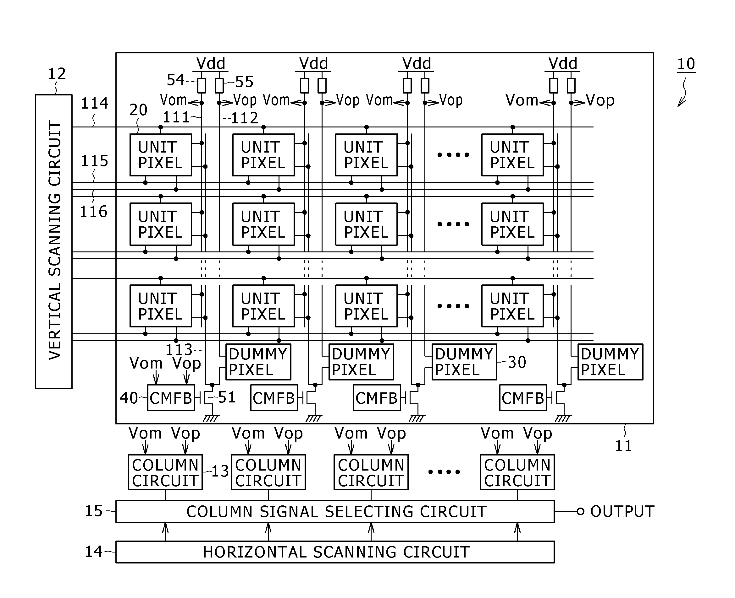
[0033]FIG. 1 is a system configuration diagram showing a configuration of a solid-state image pickup device, for example, a CMOS image sensor according to an embodiment of the present invention.

[0034]As shown in FIG. 1, a CMOS image sensor 10 of this embodiment includes a pixel array portion 11, and its peripheral circuit. In this case, the pixel array portion 11 is configured such that unit pixels each including a photoelectric conversion element (hereinafter simply referred to as “a pixel” in some cases) 20 are two-dimensionally arranged in matrix. A vertical scanning circuit 12, a plurality of column circuits 13, a horizontal scanning circuit 14, a column signal selecting circuit 15 and the like are provided as the peripheral circuit of the pixel array portion 11.

[0035]For the matrix arrangement of the unit pixels 20 in the pixel array portion 1...


PUM


Abstract

Disclosed herein is a solid-state image pickup device including: a pixel array portion; a dummy pixel; a differential circuit; a reset voltage supplying section; and a common phase feedback circuit.

Description

CROSS REFERENCES TO RELATED APPLICATIONS[0001]The present invention contains subject matter related to Japanese Patent Application JP 2007-112652 filed in the Japan Patent Office on Apr. 23, 2007, the entire contents of which being incorporated herein by reference.BACKGROUND OF THE INVENTION[0002]1. Field of the Invention[0003]The present invention relates to a solid-state image pickup device, a method of driving the same, a signal processing method for the same, and an image pickup apparatus.[0004]2. Description of the Related Art[0005]In a solid-state image pickup device, signal charges generated in a photoelectric conversion portion (light receiving portion) are transferred to a floating diffusion capacitor, and are converted into a voltage in the floating diffusion capacitor to be read out to the outside. However, it has been difficult to ensure the sufficient signal charges along with the recent miniaturization of pixels. For this reason, it has been difficult to obtain an outp...

Claims


Application Information

Patent Timeline
IPC IPC(8): G01J1/44H04N5/335H04N5/341H04N5/355H04N5/357H04N5/369H04N5/374H04N5/376
CPCG01J1/44H01L27/14603H04N5/3575H04N5/37457H04N5/365H04N5/374H04N5/37452H04N5/363H04N25/583H04N25/616H04N25/67H04N25/65H04N25/63H04N25/633H04N25/771H04N25/778H04N25/76
Inventor SAKAKIBARA, MASAKIOIKE, YUSUKE
Owner SONY CORP
Why Eureka
Try Eureka