Redundancy architecture for an integrated circuit memory

a technology of integrated circuit memory and redundancy architecture, which is applied in the field of redundancy architecture of integrated circuit memory, can solve the problems of insufficient redundant rows to repair all, increase the number of redundant rows, and increase the complexity of the circuit, so as to reduce the number of redundant columns and the effect of high multiplication width

Active Publication Date: 2008-10-23
ARM LTD
View PDF9 Cites 15 Cited by
  • Summary
  • Abstract
  • Description
  • Claims
  • Application Information

AI Technical Summary

Benefits of technology

[0034]The present technique recognizes that the shift in the number of columns to avoid a defective column does not need to be a shift corresponding to the full multiplexer size of the memory concerned. In this way, fewer redundant columns need be provided. This is a significant advantage as multiplexer width can be high, e.g. 16 or 32 bit multiplexers are common, and accordingly a large number of redundant columns would otherwise be necessary to overcome what is normally a defect within only a single column.
[0035]The redundant columns are conveniently disposed at one edge of the array of memory cells such that the shifting is toward this edge. When the integrated circuit comprises two memory arrays disposed either side of an address decoder, then each of these can include at least one redundant column and respective multiplexing circuitry such that a defective column is substituted by a redundant column from within its own memory array without having to traverse the intervening address decoder.
[0036]A frequently used way of forming integrated circuits is to use unit cell circuits which are built up into the entire integrated circuit. In this context, there is typically a minimum width of memory cells within the unit cell circuits and the multiplexer width number will be a multiple of this cell width with the main advantage of the current technique arising when this multiple is greater than two. It is convenient for the shift number to be the minimum width of memory cells within the unit circuit as this reduces the number of redundant columns which need be provided.

Problems solved by technology

A problem with redundancy architectures is that they represent an additional overhead in terms of circuit area, power consumption, complexity, and timing which has to be carried by every integrated circuit irrespective of whether or not the redundancy mechanisms for that integrated circuit are needed within the particular instance.
It is difficult to decide the number of redundant rows which should be provided in each memory bank.
If the number is too small, then there may be insufficient redundant rows to repair all the defective rows which occur within a particular memory bank.
This is particularly the case as errors tend to cluster together.
However, if too many redundant rows are provided in each memory bank, then this represents an unnecessarily high overhead.
This approach suffers from the disadvantage that the separate bank of redundant rows has to be provided with its own decoders and other support circuitry and this represents a disadvantageous additional overhead.
As previously discussed, an integrated circuit memory can also suffer from defective columns of memory cells.
The provision of a full multiplexer width group of columns that can be used as a substitute when a defective column is encountered is disadvantageous in terms of the circuit overhead consumed.

Method used


Image

  • Redundancy architecture for an integrated circuit memory
  • Redundancy architecture for an integrated circuit memory
  • Redundancy architecture for an integrated circuit memory

Examples


Embodiment Construction

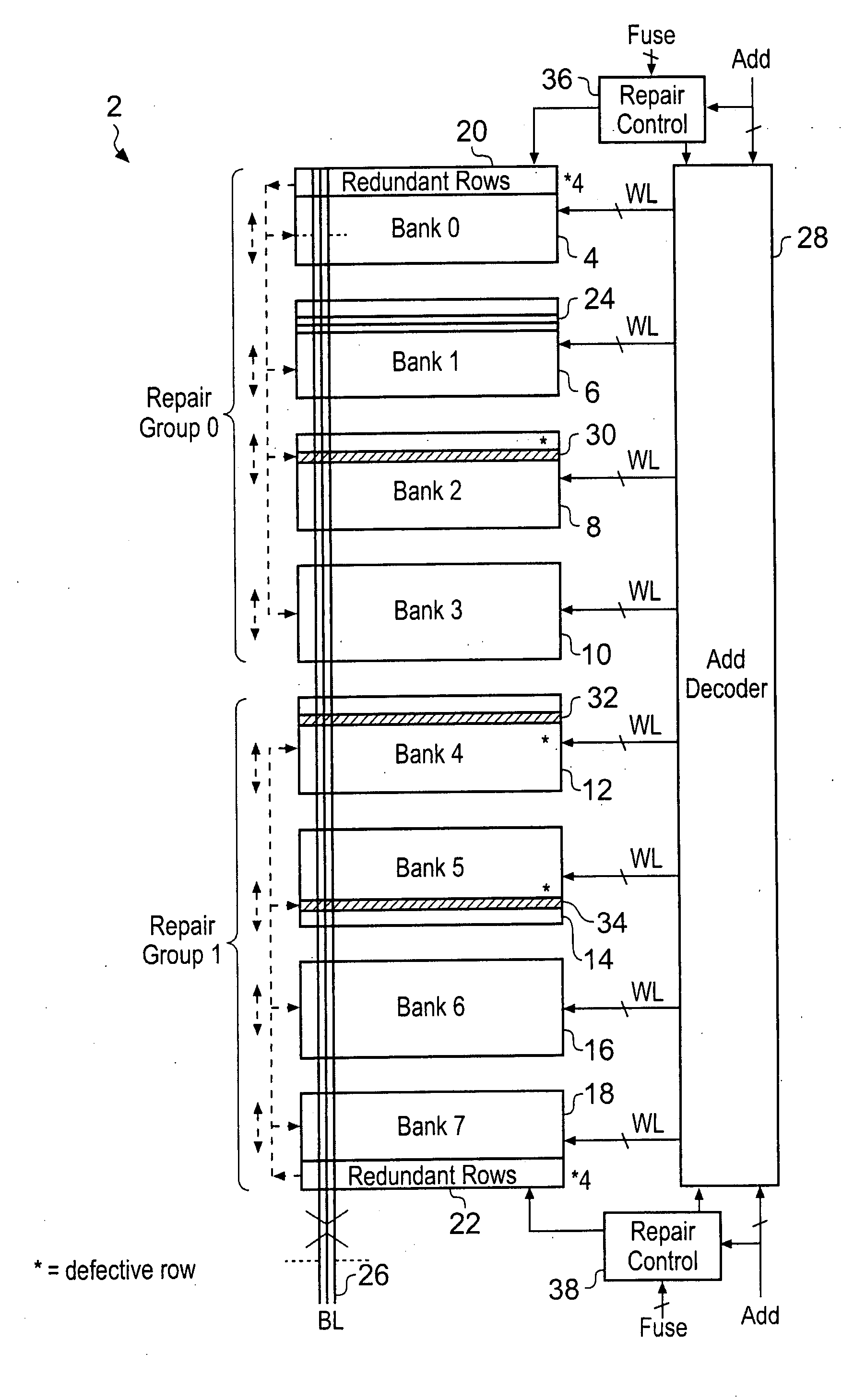
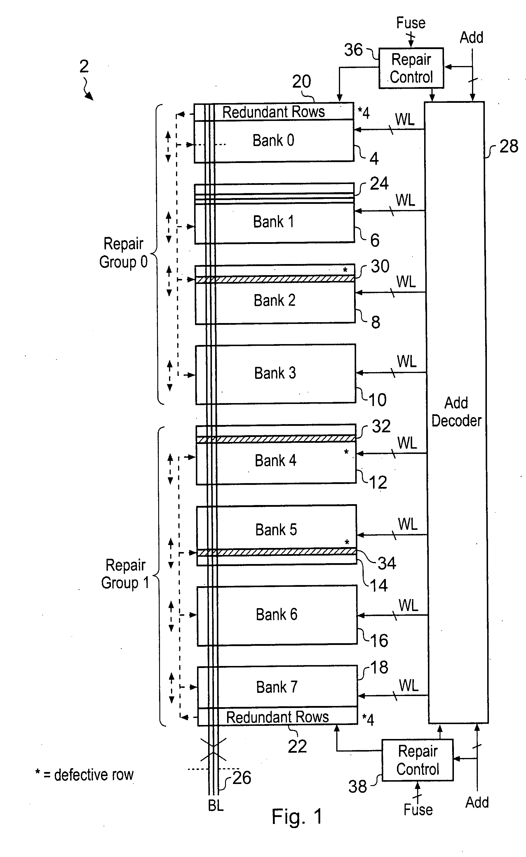
[0059]FIG. 1 schematically illustrates an integrated circuit memory 2 comprising a plurality of memory banks 4, 6, 8, 10, 12, 14, 16, 18. These memory banks 4-18 are arranged into two repair groups. The first repair group Group0 comprises memory banks 4, 6, 8, 10. The second repair group Group1 comprises memory banks 12, 14, 16, 18.

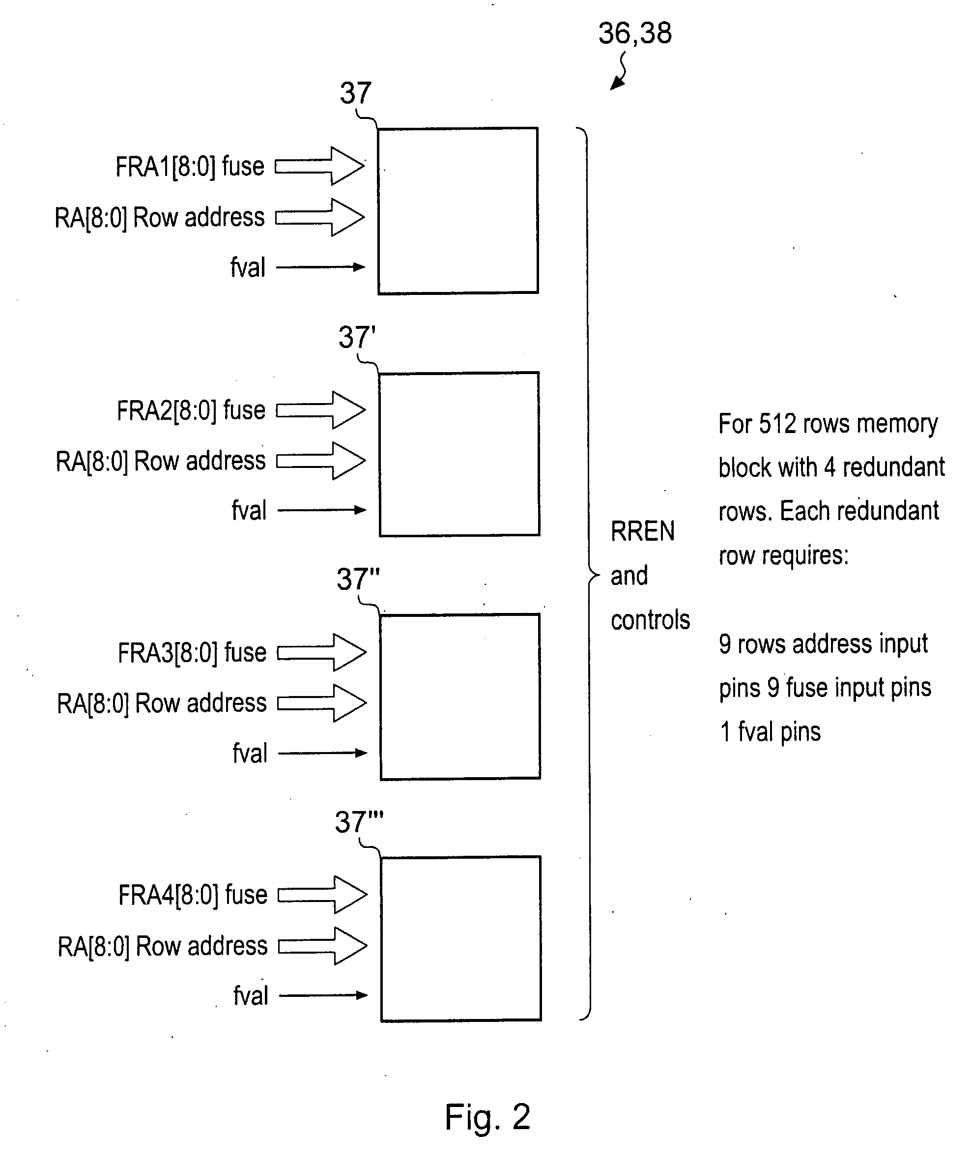
[0060]As illustrated in FIG. 1, within each of these repair groups only one of the memory banks (either memory bank 4 or memory bank 18) contains any redundant rows 20, 22. Four redundant rows are provided within memory bank 4. Four redundant rows are provided in memory bank 18. The four redundant rows 20 within the memory bank 4 may act to substitute for any of the rows of memory cells 24 within any of the memory banks 4, 6, 8, 10 which constitute Group0. It will be appreciated that each of the rows of memory cells 24 comprises a plurality of memory cells each storing one bit of data and linked to bit lines 26 via which data is read from or written to th...


PUM


Abstract

An integrated circuit memory 2 is described having multiple memory banks 4, 6, 8, 10, 12, 14, 16, 18 which are grouped into repair groups Group0, Group1. One of the memory banks 4, 18 is provided with redundant rows 20, 22 which can be used to substitute for a defective row 30, 32, 34 found within any of the memory banks within the common repair group concerned. Redundant columns of memory cells 60, 62 are also provided and these may be substituted for defective columns 66, 68 by multiplexing circuitry 56, 58. This multiplexing circuitry shifts the bit lines which are selected to form part of a bit group to access a given data bit by an amount less than the multiplexing width being supported by that multiplexing circuitry 56, 58 thereby reducing the number of redundant columns which need be provided.

Description

BACKGROUND OF THE INVENTION[0001]1. Field of the Invention[0002]This invention relates to integrated circuit memories. More particularly, this invention relates to row and column redundancy architectures for use within integrated circuit memories.[0003]2. Description of the Prior Art[0004]It is known within the field of integrated circuit memories to provide redundant memory rows and redundant memory columns within arrays of memory cells. In this way, should a defect arise which renders a row inoperative or a column inoperative, then one of the redundant rows or column may be functionally substituted for the row or column in which the defect has arisen. This type of redundancy mechanism is becoming increasingly important as process geometries scale to smaller sizes and defects within integrated circuits become statistically more likely. In this context, such redundancy mechanisms are important in maintaining a satisfactory yield.[0005]A problem with redundancy architectures is that ...

Claims


Application Information

Patent Timeline
Patent Type & Authority Applications(United States)
IPC IPC(8): G11C29/04
CPCG11C29/808G11C29/848
Inventor GAJJEWAR, HEMANGI UMAKANTWANG, KARL LIN
Owner ARM LTD
Why Eureka
Try Eureka