Semiconductor Device Having Multiple Fin Heights

a technology of semiconductor devices and fin heights, which is applied in the direction of semiconductor devices, electrical equipment, transistors, etc., can solve the problems of inability of the gate to substantially control the on and off of the transistor, and suffers from the short gate length of the transistor

Active Publication Date: 2008-10-30
TAIWAN SEMICON MFG CO LTD
View PDF13 Cites 109 Cited by
  • Summary
  • Abstract
  • Description
  • Claims
  • Application Information

AI Technical Summary

Benefits of technology

[0006]These and other problems are generally solved or circumvented, and technical advantages are generally achieved, by preferred illustrative embodiments of the present invention which provide a strained-channel transistor with lattice-mismatched region.

Problems solved by technology

Consequently, a transistor with a short gate length suffers from problems related to the inability of the gate to substantially control the on and off states of the channel.

Method used


Image

  • Semiconductor Device Having Multiple Fin Heights
  • Semiconductor Device Having Multiple Fin Heights
  • Semiconductor Device Having Multiple Fin Heights

Examples


Embodiment Construction

[0017]The making and using of the presently preferred illustrative embodiments are discussed in detail below. It should be appreciated, however, that the present invention provides many applicable inventive concepts that can be embodied in a wide variety of specific contexts. The specific illustrative embodiments discussed are merely illustrative of specific ways to make and use the invention, and do not limit the scope of the invention.

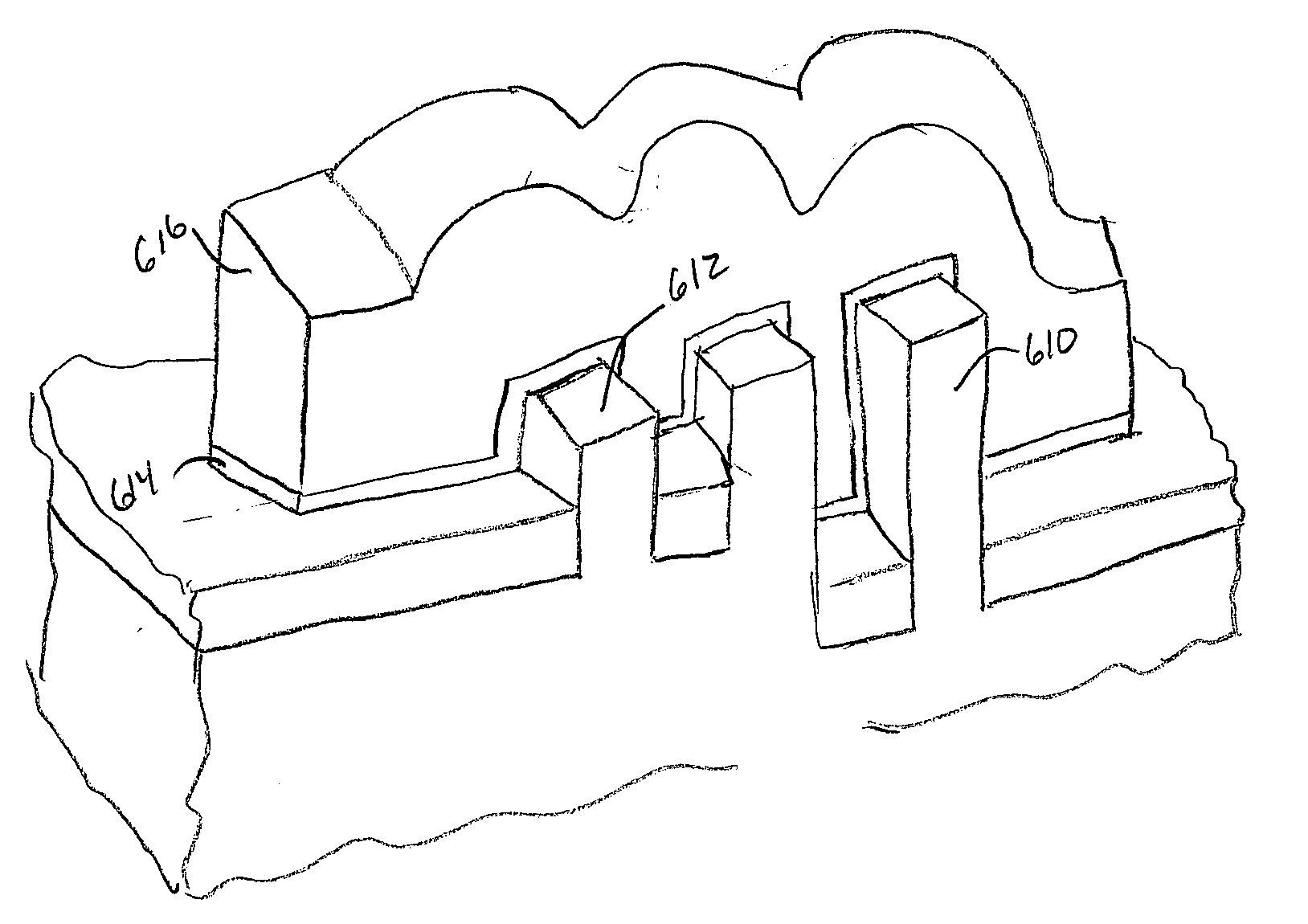
[0018]Embodiments of the present invention provide several improved methods for the formation of semiconductor devices and the resulting structures. These embodiments are discussed below in the context of forming finFET transistors having fins of different fin heights on a bulk silicon substrate. One of ordinary skill in the art will realize that embodiments of the present invention may be used with other configurations, such as, for example, omega-FETs or structures having three or more different fin heights.

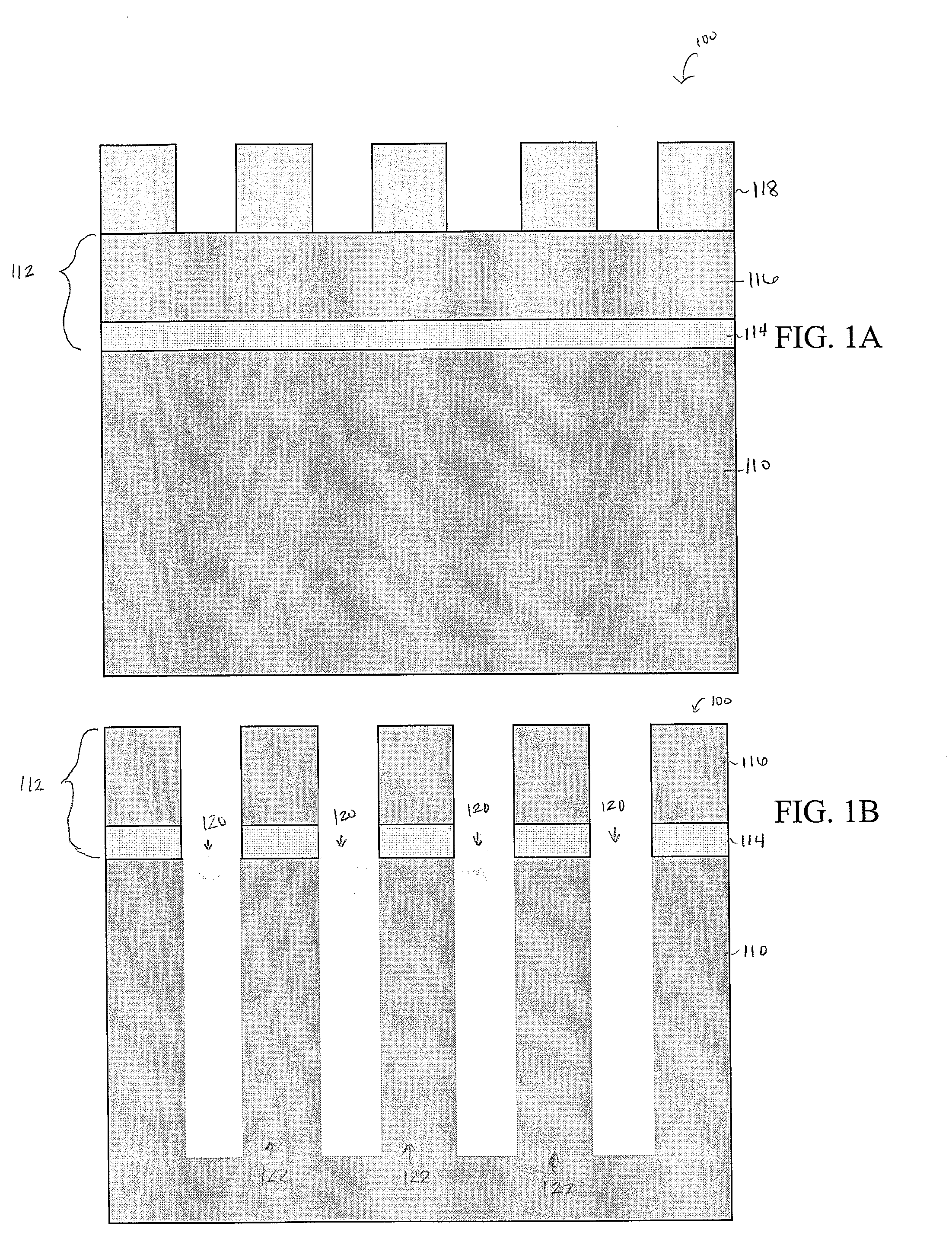
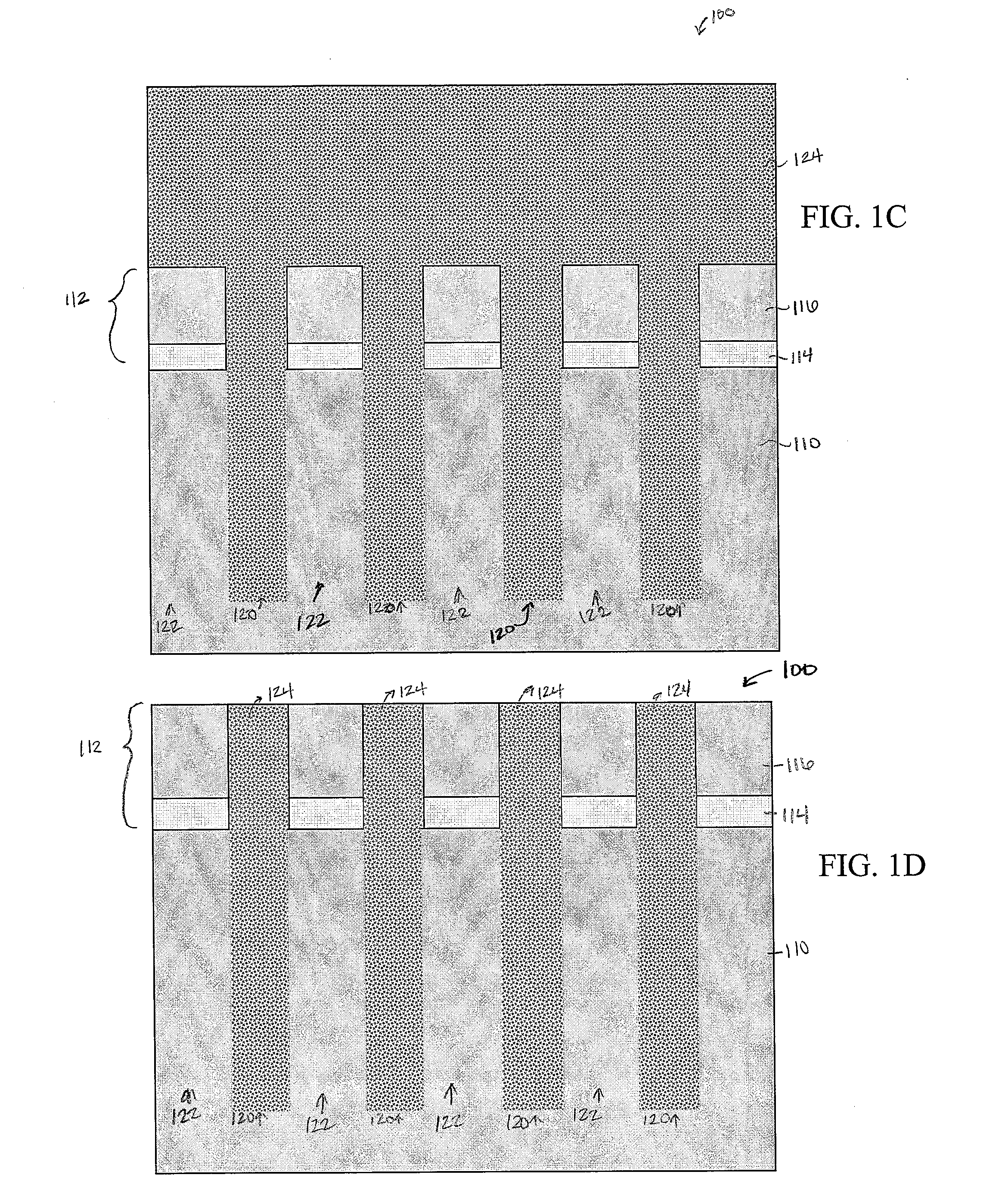
[0019]FIGS. 1a-1f illustrate a first meth...


PUM


Abstract

A semiconductor device having multiple fin heights is provided. Multiple fin heights are provided by using multiple masks to recess a dielectric layer within a trench formed in a substrate. In another embodiment, an implant mold or e-beam lithography are utilized to form a pattern of trenches in a photoresist material. Subsequent etching steps form corresponding trenches in the underlying substrate. In yet another embodiment, multiple masking layers are used to etch trenches of different heights separately. A dielectric region may be formed along the bottom of the trenches to isolate the fins by performing an ion implant and a subsequent anneal.

Description

TECHNICAL FIELD[0001]The present invention relates generally to semiconductor devices and, more particularly, to a structure of and method for forming semiconductor devices having multiple fin heights in a bulk semiconductor substrate.BACKGROUND[0002]The dominant semiconductor technology used for the manufacture of ultra-large scale integrated (ULSI) circuits is the metal-oxide-semiconductor field effect transistor (MOSFET) technology. Reduction in the size of MOSFETs has provided continued improvement in speed, performance, circuit density, and cost per unit function over the past few decades. As the gate length of the conventional bulk MOSFET is reduced, the source and drain increasingly interact with the channel and gain influence on the channel potential. Consequently, a transistor with a short gate length suffers from problems related to the inability of the gate to substantially control the on and off states of the channel.[0003]Phenomena such as reduced gate control associate...

Claims


Application Information

Patent Timeline
Patent Type & Authority Applications(United States)
IPC IPC(8): H01L29/78
CPCH01L29/66795H01L29/7851
Inventor YU, CHEN-HUAYEH, CHEN-NANHSU, YU-RUNG
Owner TAIWAN SEMICON MFG CO LTD
Why Eureka
Try Eureka