
All-Optical Devices and Methods for Data Processing

Inactive Publication Date: 2008-10-30
RAMOT AT TEL AVIV UNIV LTD +1
View PDF19 Cites 6 Cited by
  • Summary
  • Abstract
  • Description
  • Claims
  • Application Information

AI Technical Summary

Benefits of technology

[0005]There is need in the art to facilitate all-optical data processing by providing a novel method and device capable of providing very small response times of the light beams' interaction zone medium, and enabling to operate with relatively low light intensity and relatively small size of the interaction zone.
[0006]The present invention solves the above problem by providing an all-optical data processing method and device that utilize light propagation through a linear-medium. The dimensions of such an all-optical processor may be similar to those of a Very Large Scale Integration (VLSI) circuit (about 2 cubic micrometer for logical AND gate), but the operation is more than 10,000 times faster and approaches a few tens of T-Hz. The device of the present invention facilitates realization of various logic functions that may be used in a fast RAM module, a femto second pulse generator, a light amplitude / phase modulator, a coder / decoder, an optical switch, an analog / digital or digital / analog converter, and in other data processing components. The rate of the data processing is close to the rate of light (100 THZ).
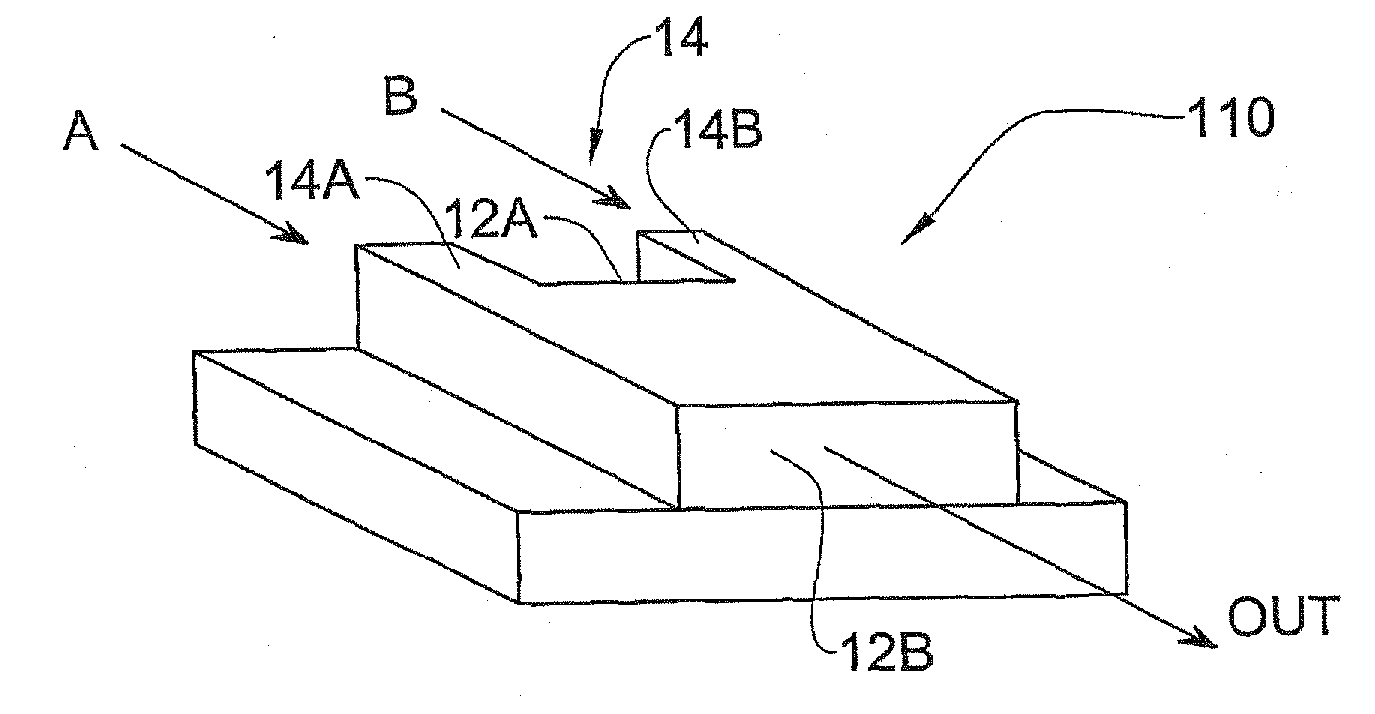
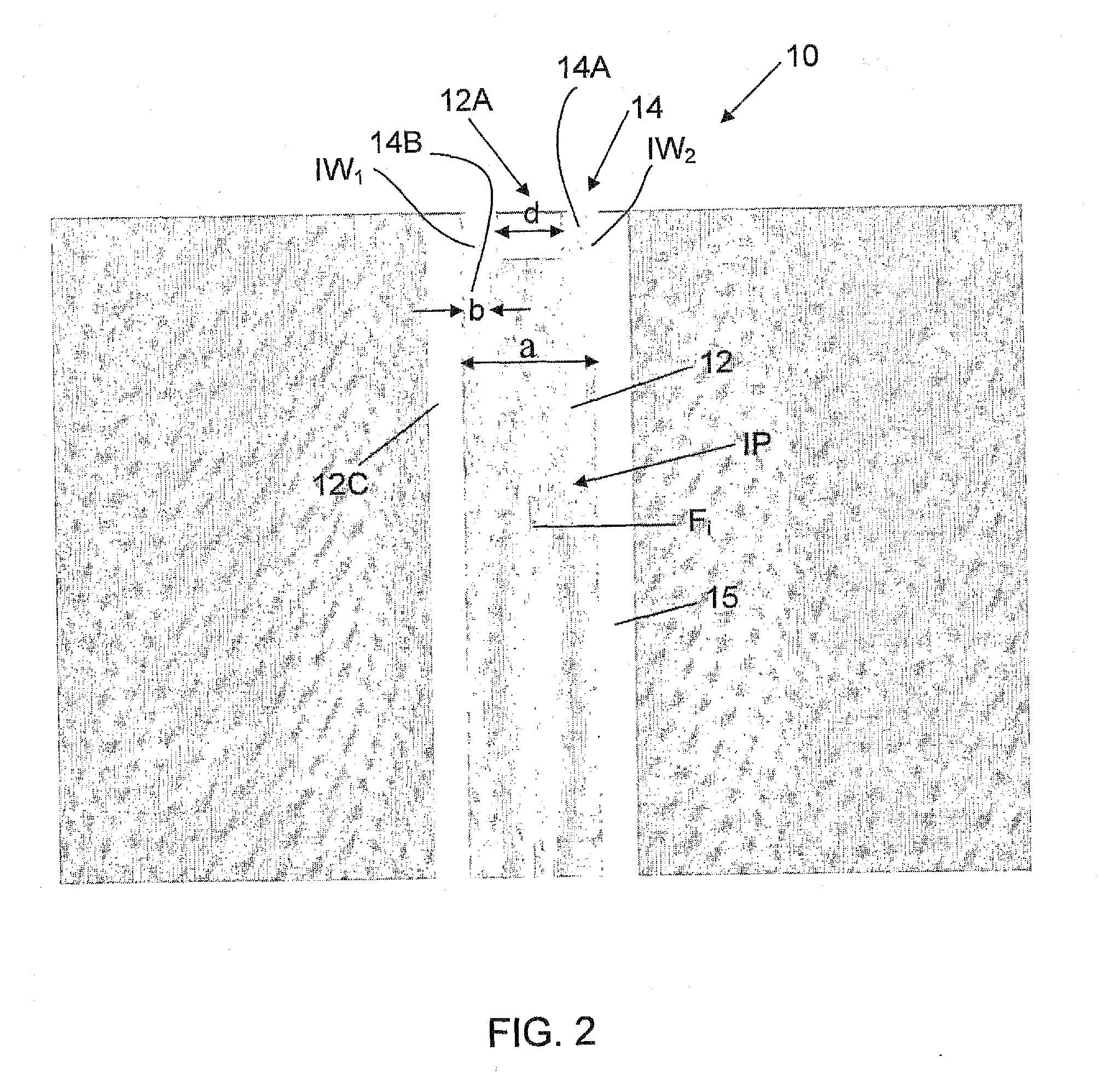
[0039]According to yet another aspect of the invention, there is provided a method for all-optical data processing, the method comprising inputting light through at least one input aperture of a cross-sectional dimension b into an optical waveguide unit made of linear media having a cross-sectional dimension a larger than b, thus providing multiple total internal reflections of the light passing through the waveguide unit and to cause diffraction-based interactions between reflected light components of the input light, thereby determining an interference pattern resulting from said interaction; and facilitating light output from the waveguide unit at a desired location relative to features of the pattern to provide at the output an appropriate modulation of at least one light parameter selected from a phase of the input light and an amplitude of the input light.

Problems solved by technology

This results in interference, namely the summation of the light fields (which is a linear function of the input field) at the point of intersection.

Method used


Image

  • All-Optical Devices and Methods for Data Processing
  • All-Optical Devices and Methods for Data Processing
  • All-Optical Devices and Methods for Data Processing

Examples


Embodiment Construction

[0061]The present invention provides various configurations of an all-optical data processing device that has a significantly reduced volume in comparison with the known devices of the kind specified, and which relieves the dependence of the operation rate on a response time of an optical medium of the device through which light propagates. The present invention also provides a method for all-optical data processing and manipulation based upon the fact that several light beams that interact among themselves in a linear-medium optical waveguide generate focuses at different positions in the device, that depend on the phase and the spatial distribution of the input light. This property allows for constructing a device that is independent of the materials response time. Known approaches for data processing operation use phase and / or amplitude modulation of input data. The devices of the present invention may be designed for such types of modulation.

[0062]Thus, the present invention pro...


PUM


Abstract

An all-optical device for data processing is presented. The device comprises at least one optical waveguide unit (10) made of linear media and configured to provide multiple total internal reflections of light passing therethrough, the waveguide unit (10) comprising a waveguide portion (11) for interaction between reflected light components of input light; an input aperture arrangement (14) formed by at least one input aperture at an input facet of the waveguide portion (11); and an output aperture arrangement forme by at least one output aperture at an output facet of the waveguide portion. The geometry of the input aperture arrangement and the waveguide portion is selected so as to determine an interference pattern resulting from a diffraction-based interaction between light components of a predetermined wavelength while the light components propagate through the waveguide portion, a location of the at least one output aperture relative to features of the interference pattern being selected to provide at the output an appropriate modulation of at least one parameter of the input light.

Description

FIELD OF THE INVENTION[0001]This invention relates to all-optical devices and methods for data processing, including optical computing, information and communication systems and logic elements for use therein.BACKGROUND OF THE INVENTION[0002]Optical techniques for data processing are known as those providing ultra fast data processing capabilities that are independent of electrical cross talk and induced noises. Existing all-optical devices for data processing are based on the use of non-linear effects achieved by light propagation through a non-linear medium. The non-linear effect is thus obtained via light interaction with electrons of the material due to non-linear oscillations of electrons.[0003]Such devices are described for example in U.S. Pat. Nos. 5,150,248; 5,373,381 and 5,463,485 which disclose optical computing systems, communication systems, and logic elements using cross-phase modulation based optical processors to alter and control, either alone or simultaneously, the ...

Claims


Application Information

Patent Timeline
IPC IPC(8): G02F3/00G02F1/035
CPCG02B6/2813G06E3/001
Inventor ZALEVSKY, ZEEVROUDNITSKI, ARKADINATAN, MENACHEM
Owner RAMOT AT TEL AVIV UNIV LTD
Learn More