

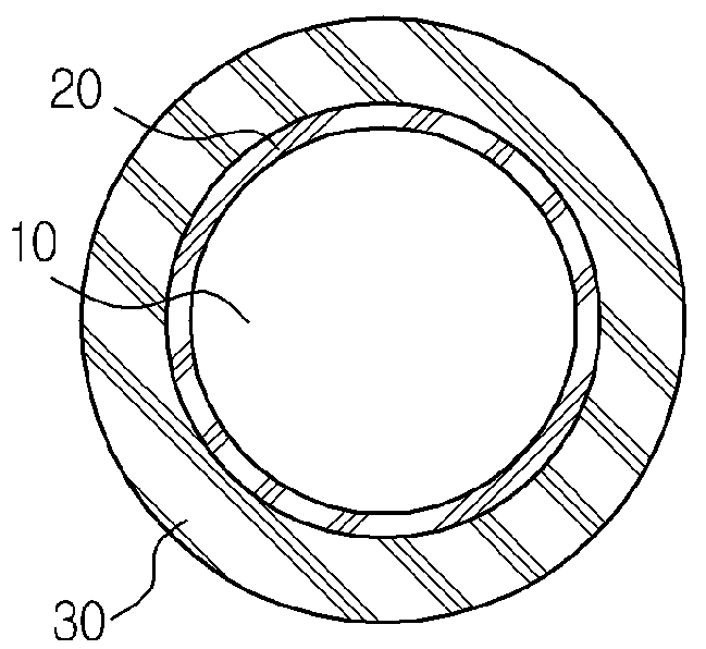
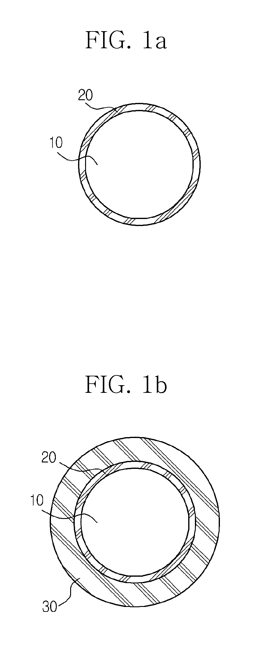
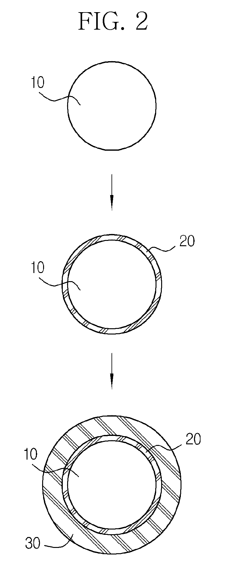
Nanocrystal, method for preparing the same and electronic device comprising the same
a nanocrystal and nanocrystal technology, applied in the field of nanocrystal, can solve the problems of difficult growth of nanocrystals, poor quality of nanocrystals, and difficult to synthesize nanocrystals, and achieve the effect of improving luminescence properties and color purity
- Summary
- Abstract
- Description
- Claims
- Application Information
AI Technical Summary
Benefits of technology
Problems solved by technology
Method used
Image

Examples
preparation example
Synthesis of an InP nanocrystal core
[0064]Indium acetate (0.058 g, 0.2 mmol) and oleic acid (0.118 g, 0.6 mmol) were dissolved in 10 g of octadecene (ODE) to prepare an indium precursor solution. The indium precursor solution was heated at about 120° C. until it became clear. The indium precursor solution was allowed to react under vacuum for about 90 min. The solution was then washed three times with nitrogen and heated to about 300° C. under a nitrogen atmosphere. Separately, 0.1 mmol of tris-((trimethylsilyl)phosphine) was dissolved in 2 g of ODE to prepare a phosphine precursor solution. The phosphine precursor solution was added all at once to the reaction mixture being heated at about 300° C. After about a 20° C. or greater drop in temperature, the reaction mixture was cooled to about 270° C. and allowed to react for an additional 2 hours in order to produce an indium phosphate (InP) nanocrystal core.
[0065]FIG. 3A is a graph showing the UV absorbance for the InP nanocrystal co...
example 1
Synthesis of an InP / Se / ZnS nanocrystal
[0066]Indium acetate (0.07 mmol) and oleic acid (0.3 mmol) were mixed with 10 g of octadecene (ODE) followed by stirring under vacuum at a temperature of about 120° C. Next, 0.05 mmol of tris-((trimethylsilyl) phosphine) and 1 mL of ODE were fed to the mixture and heated at about 250° C. The reaction mixture was allowed to react for about 20 min. After completion of the reaction, a Se-Top solution (0.1 M, 0.02 mL) was added to the reaction mixture and allowed to react for about 30 min. Then, a solution containing 0.2 mmol Zn—OA was fed to the resulting mixture and allowed to react with stirring for about one hour. After the reaction temperature was elevated to about 300° C., an S-TOP (0.4 M, 1 mL) was fed to the mixture and allowed to react for about one hour to yield an InP / Se / ZnS nanocrystal.
[0067]FIG. 4A shows the UV-Vis absorption spectrum for the InP / Se / SnS nanocrystal, and FIG. 4B shows the photoluminescence spectrum for the InP / Se / ZnS nan...
example 2
Synthesis of an InP / S / ZnS nanocrystal
[0070]Indium acetate (0.07 mmol) and oleic acid (0.3 mmol) were mixed with 10 g of octadecene (ODE) followed by stirring under vacuum to about 120° C. Next, 0.05 mmol of tris-((trimethylsilyl) phosphine) and 1 mL of ODE were fed to the mixture and heated at about 250° C. The reaction mixture was allowed to react for about 20 min. After completion of the reaction, a S-Top solution (0.1 M, 0.02 mL) was added to the reaction mixture and allowed to react for about 30 min. After a solution containing 0.2 mmol Zn—OA was fed to the resulting mixture, the mixture was allowed to react for about 30 min while the reaction temperature was elevated to about 300° C. Next, 1 mL of 0.4M Se / TOP was fed to the reaction mixture and allowed to react for about one hour to yield an InP / S / ZnS nanocrystal. FIG. 6 shows the photoluminescence spectrum for the InP / S / ZnS nanocrystal. The quantum efficiency of the InP / S / ZnS nanocrystal was determined to be about 41% and the ...
PUM
| Property | Measurement | Unit |
|---|---|---|
| thickness | aaaaa | aaaaa |
| thickness | aaaaa | aaaaa |
| thickness | aaaaa | aaaaa |
Abstract
Description
Claims
Application Information