Signal Converting Circuit

a conversion circuit and signal technology, applied in the direction of logic circuit coupling/interface arrangement, pulse technique, instruments, etc., can solve the problems of increased circuit area, increased current consumption, difficult to achieve high-speed circuit operation, etc., to achieve reduced circuit area, higher-speed operation, and reduced current consumption

Active Publication Date: 2008-11-06
THINE ELECTRONICS
View PDF2 Cites 4 Cited by
  • Summary
  • Abstract
  • Description
  • Claims
  • Application Information

AI Technical Summary

Benefits of technology

[0026]As explained above, by means of a signal conversion circuit of this invention, the circuit area can be decreased while reducing current consumption, and higher-speed operation becomes possible.

Problems solved by technology

In the amplifier circuit described in Patent Reference 1, because the operating speed is constrained by the transistor load capacitance, there is the problem that high-speed circuit operation is difficult to achieve.
Further, two differential amplifier circuits must be prepared in order to convert the input common-mode voltage, and so there are the problems of an increase in circuit area and greater current consumption.

Method used


Image

  • Signal Converting Circuit
  • Signal Converting Circuit
  • Signal Converting Circuit

Examples


first embodiment

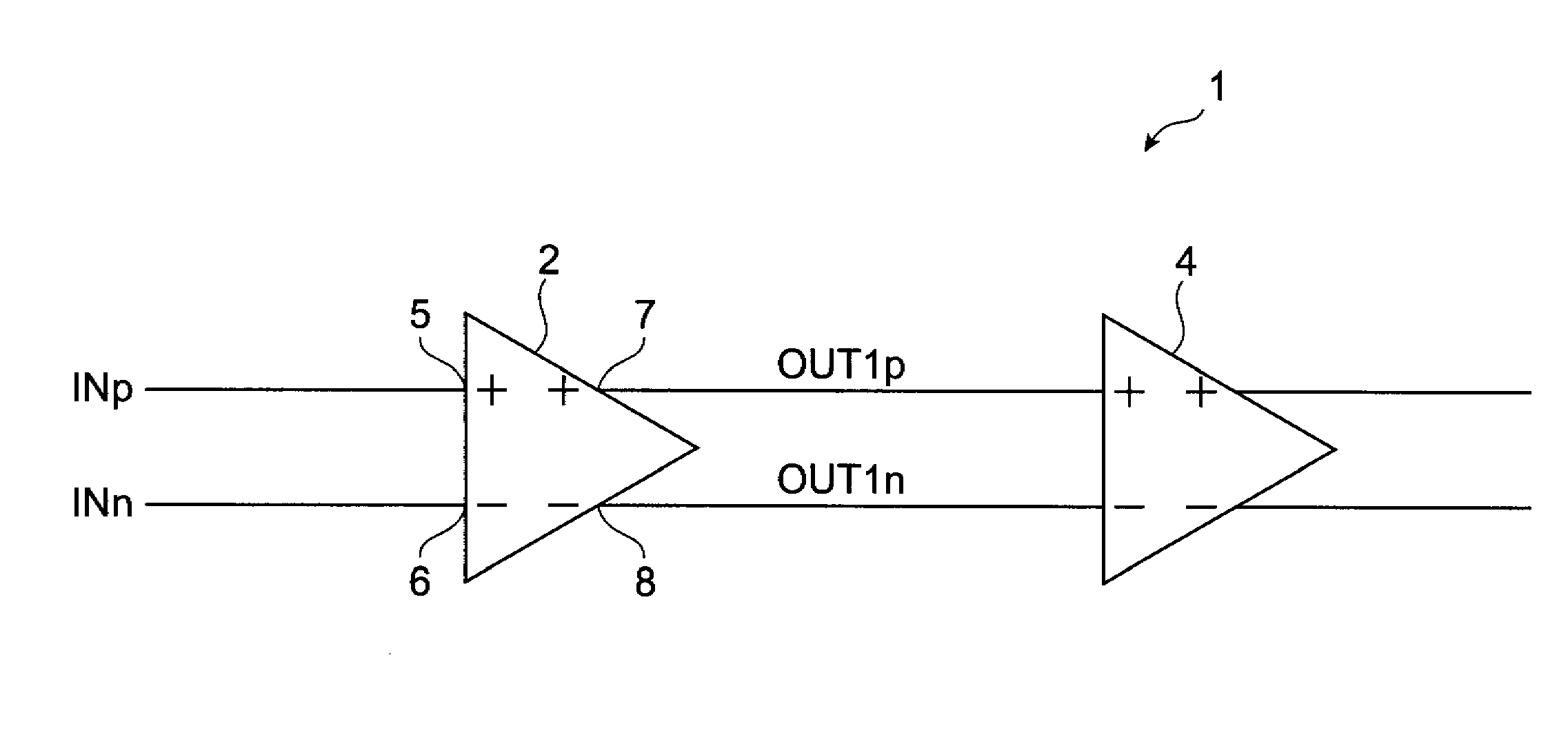
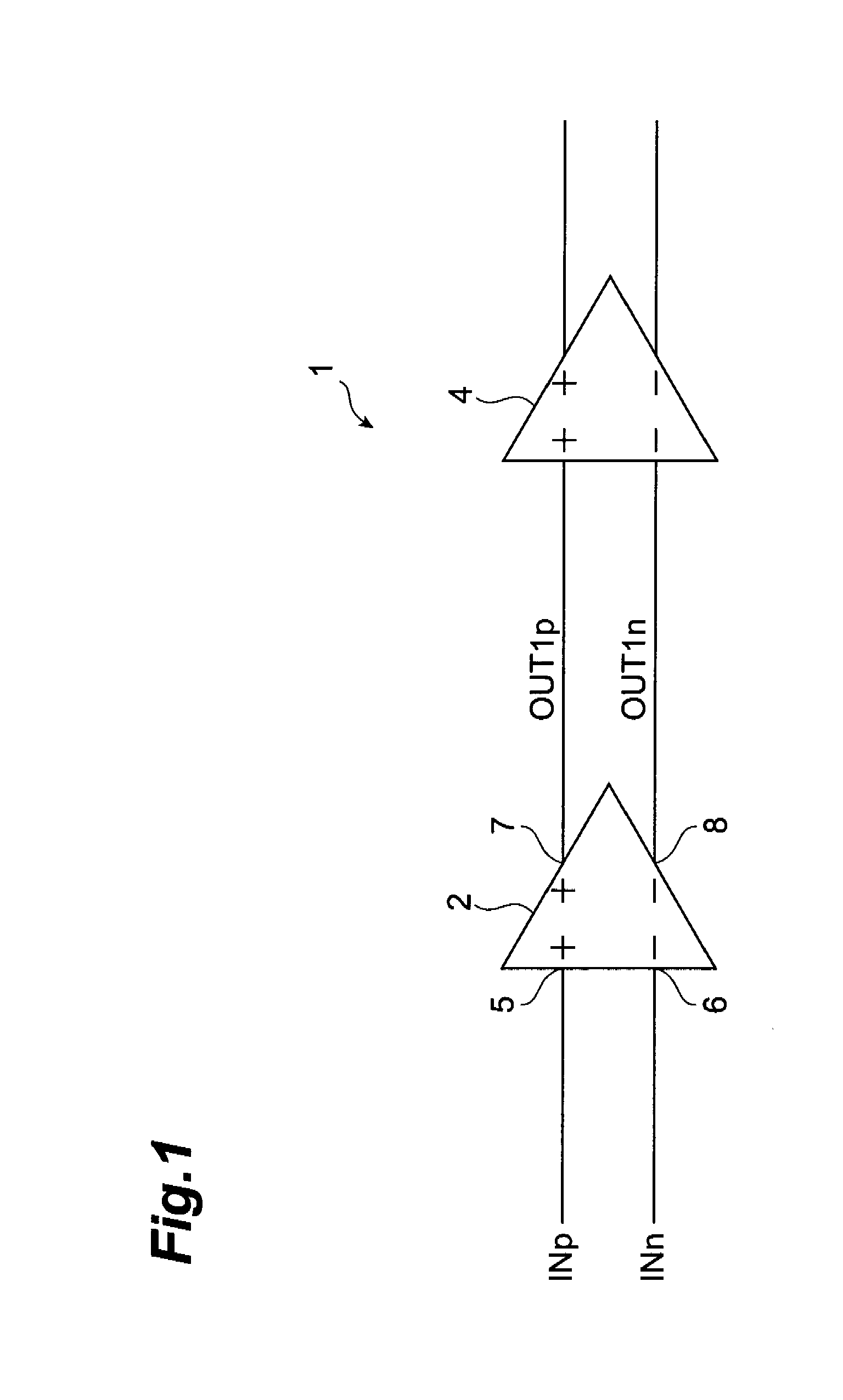
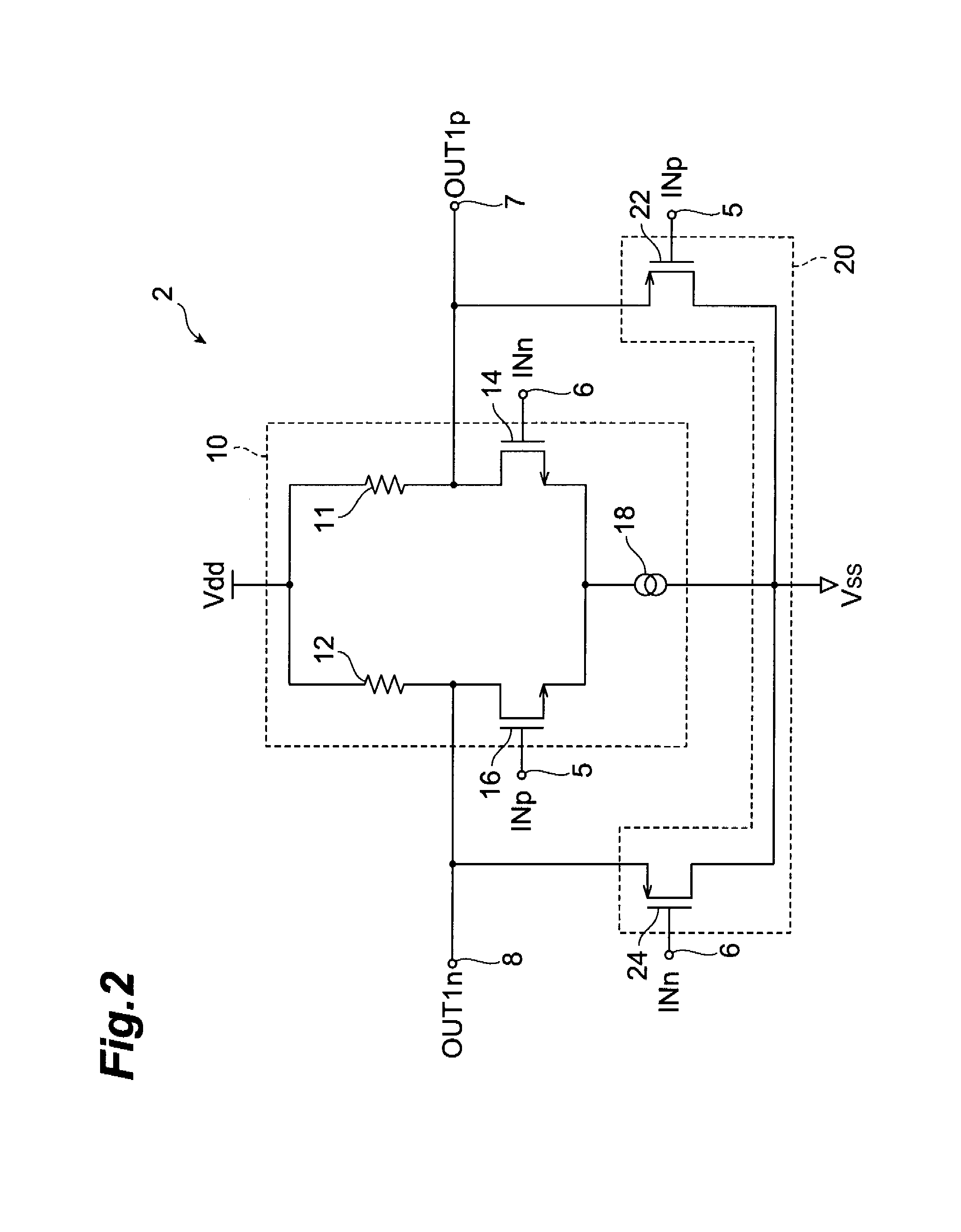
[0062]FIG. 1 shows the configuration of a rail-to-rail type differential amplifier circuit, comprising the signal conversion circuit of a first embodiment of the invention. This rail-to-rail circuit 1 is a differential amplifier circuit which acquires input signals over a broad range of common-mode voltages, performs prescribed amplification and outputs the result, and is for example used in LVDS reception device. The rail-to-rail circuit 1 comprises a signal conversion circuit 2, which converts the common-mode voltage level of input differential voltage signals, and a differential amplifier circuit 4 which amplifies the converted differential voltage signals converted to a prescribed common-mode voltage level.

[0063]Differential voltage signals INp and INn are input to the first input terminal 5 and second input terminal 6 respectively of the signal conversion circuit 2. The signal conversion circuit 2 converts the common-mode voltage level of the differential voltage signals INp an...

second embodiment

[0077]Next, a second embodiment of the invention is explained. FIG. 4 is a circuit diagram of the signal conversion circuit of the second embodiment of the invention. Similarly to the above-described signal conversion circuit 2, the signal conversion circuit 30 is a circuit used in rail-to-rail type differential amplification circuits, and converts the common-mode voltage level of input differential voltage signals into a prescribed common-mode voltage level. The differential voltage signals INp and INn are input to a first input terminal 31 and second input terminal 32, respectively, of the signal conversion circuit 30. The signal conversion circuit 30 converts the common-mode voltage level of the differential voltage signals INp and INn to the prescribed common-mode voltage level, and outputs the differential voltage signals OUT2p and OUT2n to the first output terminal 33 and second output terminal 34, respectively. The differential amplification circuit 4 shown in FIG. 1 acquires...

third embodiment

[0092]FIG. 5 is a circuit diagram showing the signal conversion circuit of a third embodiment of the invention. The signal conversion circuit 2A shown in FIG. 5 differs from the first embodiment in that, in place of the source follower portion 20 in the signal conversion circuit 2, the source follower portion 20A is comprised. Otherwise the configuration of signal conversion circuit 2A is similar to that of signal conversion circuit 2.

[0093]The source follower portion 20A differs from the source follower portion 20 in further comprising a third NMOS transistor 23 and fourth NMOS transistor 25. Otherwise the configuration of the source follower portion 20A is similar to that of the source follower portion 20.

[0094]The drain electrode of the third NMOS transistor 23 is connected to the first output terminal 7, and the source electrode of the third NMOS transistor 23 is connected to the source electrode of the first PMOS transistor 22. A first bias voltage is input to the gate electrod...


PUM


Abstract

A signal conversion circuit 2 comprises a differential amplifier portion 10 and a source follower portion 20. When differential voltage signals INp and INn are input to a first input terminal 5 and second input terminal 6 respectively, operations occurs either in a mode in which only the differential amplifier portion 10 operates, or a mode in which both the differential amplifier portion 10 and the source follower portion 20 operate, or a mode in which only the source follower portion 20 operates, according to the levels of the differential voltage signals INp and INn. The differential amplifier portion 10 and source follower portion 20 have fewer components compared with a circuit comprising two differential amplifier circuits. By this means, the circuit area can be reduced, and in addition current consumption can be reduced. Also, because the source follower portion 20 performs non-inverting amplification of the differential voltage signals INp and INn, high-speed operation is possible.

Description

TECHNICAL FIELD[0001]This invention relates to a signal conversion circuit, and in particular relates to a signal conversion circuit which converts the common-mode voltage of differential voltage signals.BACKGROUND ART[0002]In a reception device which receives differential voltage signals, a common-mode voltage offset which depends on the transmission device and on the state of the transmission line, and a broad input common-mode voltage to accommodate a low-voltage interface, are sought. Such a reception device is provided with a signal conversion circuit to convert the common-mode voltage of input differential signals into a prescribed voltage level. For example, in an LVDS (Low-Voltage Differential Signaling) reception device which transmits and receives digital signals by changing the current direction in a pair of resistance-terminated differential transmission lines, a signal conversion circuit converts the input common-mode voltage into a voltage which is higher than the sum ...

Claims


Application Information

Patent Timeline
Patent Type & Authority Applications(United States)
IPC IPC(8): H03L5/00H03F3/45
CPCH03F1/223H03F3/345H03F3/45183H03F3/45475H03F3/505H03F2203/45288H03F2203/45352H03F2203/45612H03F2203/45652H03F2203/45702H03K17/04106H03F3/34H03F3/45H03K19/0175
Inventor MIURA, SATOSHIMASUDA, MAKOTO
Owner THINE ELECTRONICS
Why Eureka
Try Eureka