

Novel Class of Ferromagnetic Semiconductors
a technology of ferromagnetic semiconductors and semiconductors, applied in the field of new ferromagnetic semiconductors, can solve the problems of unsuitable devices, soft ferromagnetic semiconductors (fss), lack of suitable room temperature, etc., and achieve the effect of enhancing the functionality of microelectronic devices and substantial commercial value in the marketpla
- Summary
- Abstract
- Description
- Claims
- Application Information
AI Technical Summary
Benefits of technology
Problems solved by technology
Method used
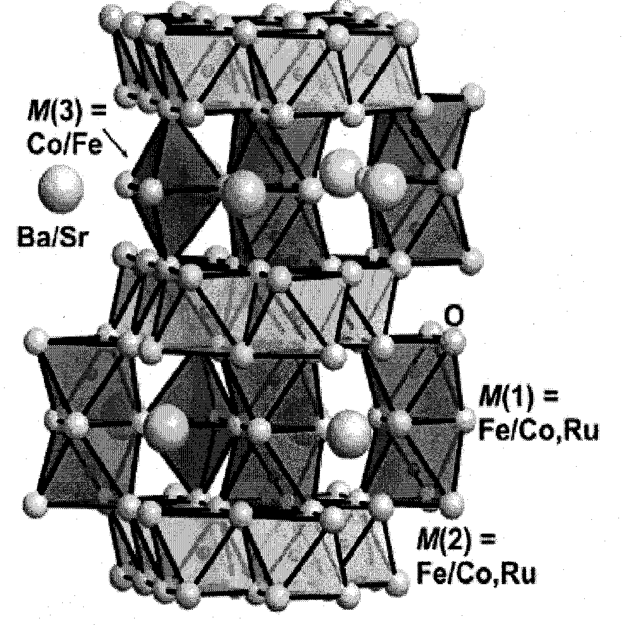
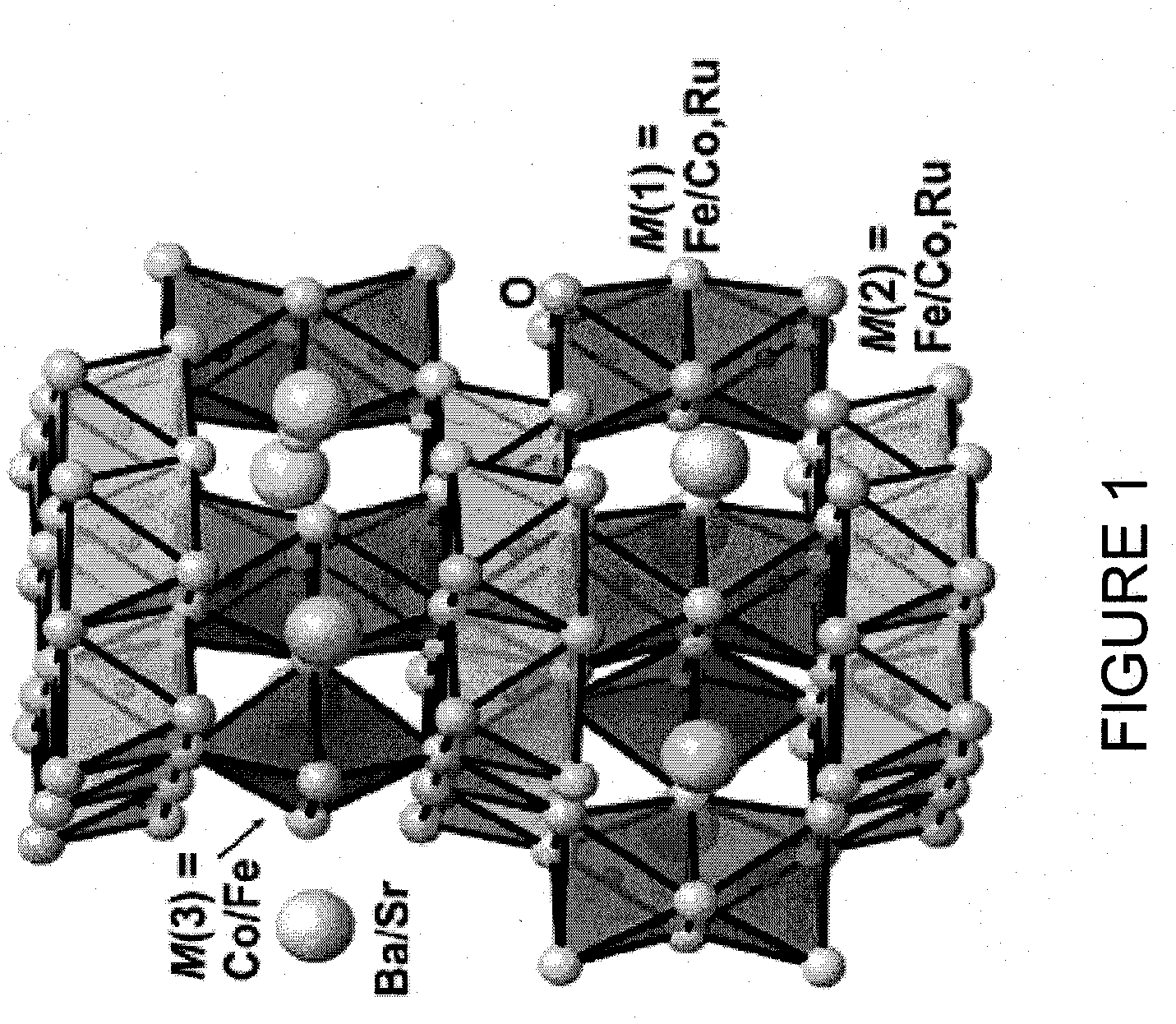
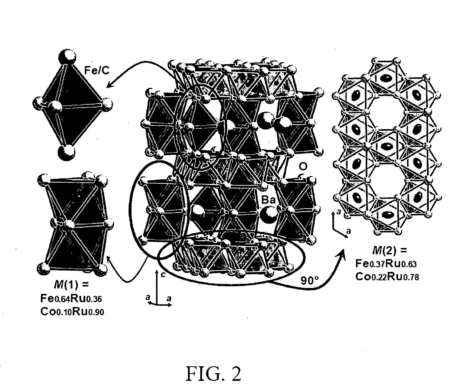
Image

Examples
Embodiment Construction
[0082]For preparation of BaFe3.39(5)Ru2.61(5)O11, 11.3 mmol BaCo3, 3.40 mmol RuO2 and 1.39 mmol Fe2O3 were mixed with about 1.5 g of BaCl2, which was used as an agent to initiate crystal growth. The resulting powders were heated to 1350° C. and kept at this temperature for 70 hr. Then the furnace was slowly cooled (˜50° C. / hr.) to room temperature. Black, hexagonal, single-crystalline platelets with maximal sizes of 2 mm and a thickness of about 0.05 mm were obtained.
[0083]Starting materials for BaCo1.85(6)Ru4.15(6)O11 were 11.3 mmol BaCo3, 3.40 mmol RuO2, and 1.30 mmol CO3O4. After addition of BaCl2, this mixture was treated in the identical manner as for the Fe compound.
[0084]Single crystal samples of SrFe2.6Ru3.4O11 were prepared by mixing 0.26 mol. % Fe2O3, 0.52 mol. % RuO2 and 0.39 mol. % SrCl2. The powder mixture was heated in air at ambient pressure to 1300° C. and kept at this temperature of 50 hr. The furnace was cooled to 1000° C. for 4 hr. and then switc...
PUM
| Property | Measurement | Unit |
|---|---|---|
| Curie temperature | aaaaa | aaaaa |
| ferromagnetic ordering temperature Tc | aaaaa | aaaaa |
| coercive field | aaaaa | aaaaa |
Abstract
Description
Claims
Application Information