Light-emitting element and method for manufacturing the same

a technology of light-emitting elements and manufacturing methods, which is applied in the direction of laser optical resonator construction, semiconductor lasers, lasers, etc., can solve the problems of inability to achieve desirable effects, inability to achieve far-field pattern defects, etc., and achieve easy and accurate control of the width of the current constriction region, the effect of reducing the rate of insulating treatmen

Active Publication Date: 2008-11-13
SONY CORP
View PDF2 Cites 37 Cited by
  • Summary
  • Abstract
  • Description
  • Claims
  • Application Information

AI Technical Summary

Benefits of technology

[0042]In the second embodiment of the present invention, a second electrode is disposed on the top face of a protrusion located outside the edge of the top face of a second compound semiconductor layer constituting the mesa structure. Consequently, unlike in the related art, it is not always necessary to provide the second electrode in the shape of a ring on the periphery of the top face of the second compound semiconductor layer in the mesa structure. Therefore, even if a large displacement occurs between a current constriction region disposed in the mesa structure and the second electrode, a current can be reliably supplied from the second electrode to the second compound semiconductor layer in the mesa structure, and moreover, the possibility is low that light from the active layer is blocked by the second electrode provided outside the edge of the top face of the second compound semiconductor layer. Broadly speaking, the second embodiment of the present invention includes the first embodiment of the present invention. That is, depending on the shape of the protrusion in the second embodiment of the present invention, such a protrusion can have the same shape, configuration, and structure as those of the wall structure or the bridge structure in the first embodiment of the present invention.
[0043]Furthermore, in the third embodiment of the present invention, a plurality of point-like holes which reach at least an insulation region are disposed so as to extend in the lamination direction. Here, the formation of the insulation region starts from sidewalls of the holes, and each insulation region expands outward with the corresponding hole serving as a center. Consequently, the amount of the species to be used in insulating treatment, such as an oxidizing species, per unit area of the insulation region front decreases as the insulating treatment progresses, and thus the rate of the insulating treatment decreases. Therefore, even if the current constriction structure is small, it is possible to easily and accurately control the width of the current constriction region or the width of the insulation region. Moreover, since merely the plurality of point-like holes are formed, the formation of the current constriction region itself is easy. Consequently, it is possible to satisfy requirements for reduction in size of mesa structures and size of current constriction regions. At the same time, it is possible to provide the second electrode on the top face of the second compound semiconductor layer sufficiently apart from the space above the current constriction region so that light from the active layer is not blocked by the second electrode even if a large displacement occurs between the current constriction region and the second electrode disposed on the top face of the second compound semiconductor layer.
[0044]Furthermore, in any of the embodiments of the present invention, since the area of the second electrode to be provided on the top face of the second compound semiconductor layer can be decreased, it is possible to decrease a capacitance, i.e., parasitic capacitance, formed by the second electrode, the insulation region, and the first electrode.

Problems solved by technology

If such a phenomenon occurs, in addition to the loss of optical output, a problem arises in which a defect occurs in the far-field pattern (FFP), which is an important parameter when emitted light is collected by a lens or guided to an optical fiber.
However, such an approach is not desirable because it is difficult to satisfy requirements for reduction in size of mesa structures and reduction in size of current constriction regions, or because it is difficult to form very small current constriction regions.

Method used


Image

  • Light-emitting element and method for manufacturing the same
  • Light-emitting element and method for manufacturing the same
  • Light-emitting element and method for manufacturing the same

Examples


example 1

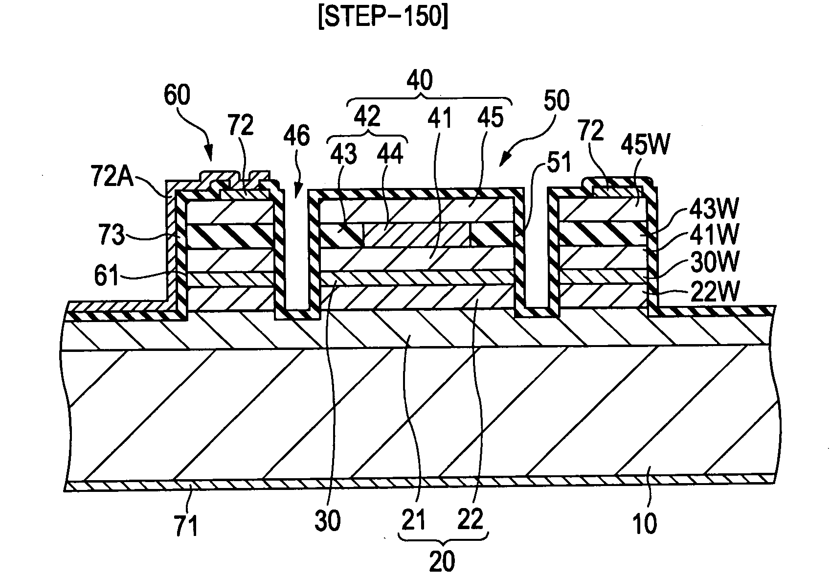
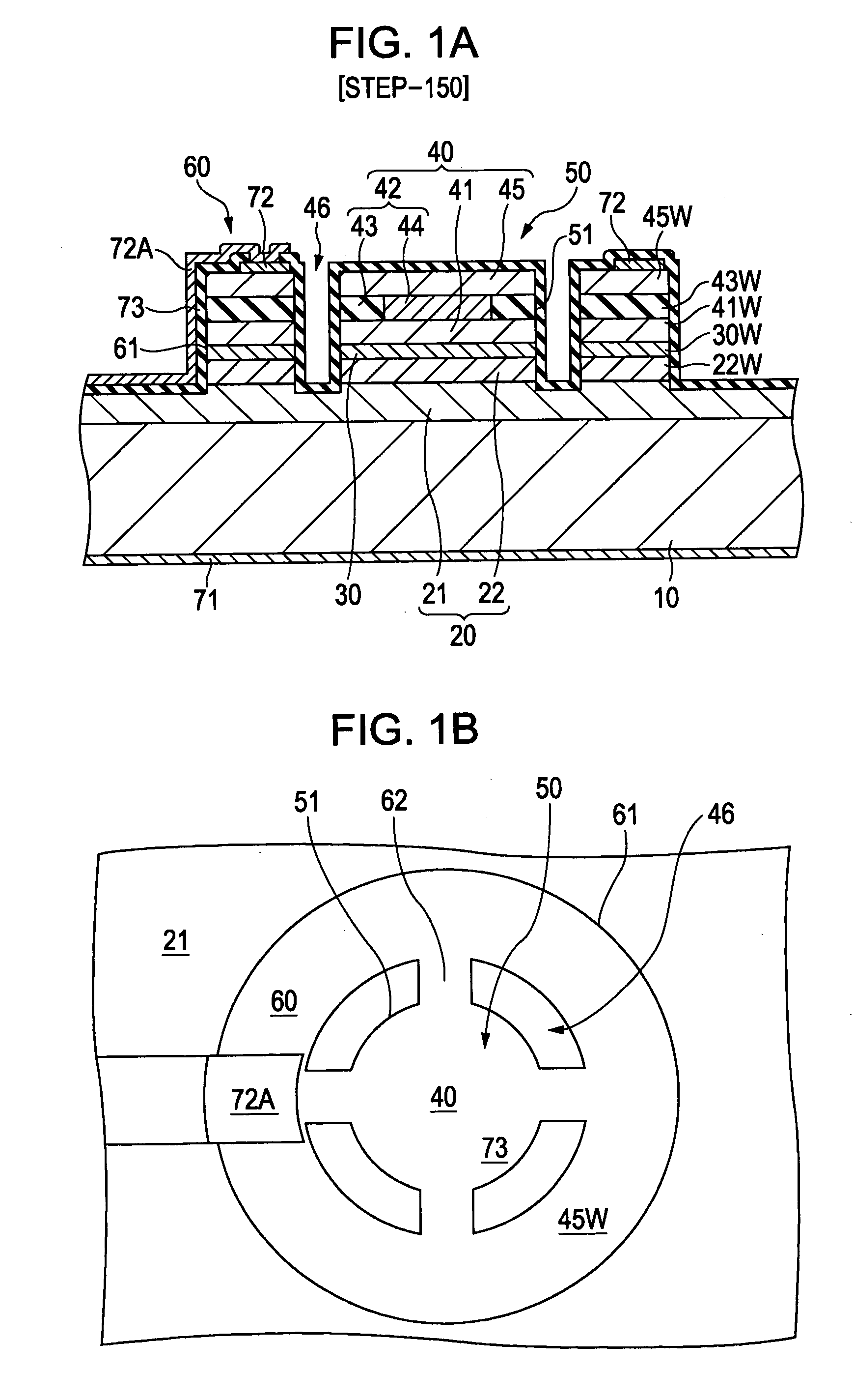
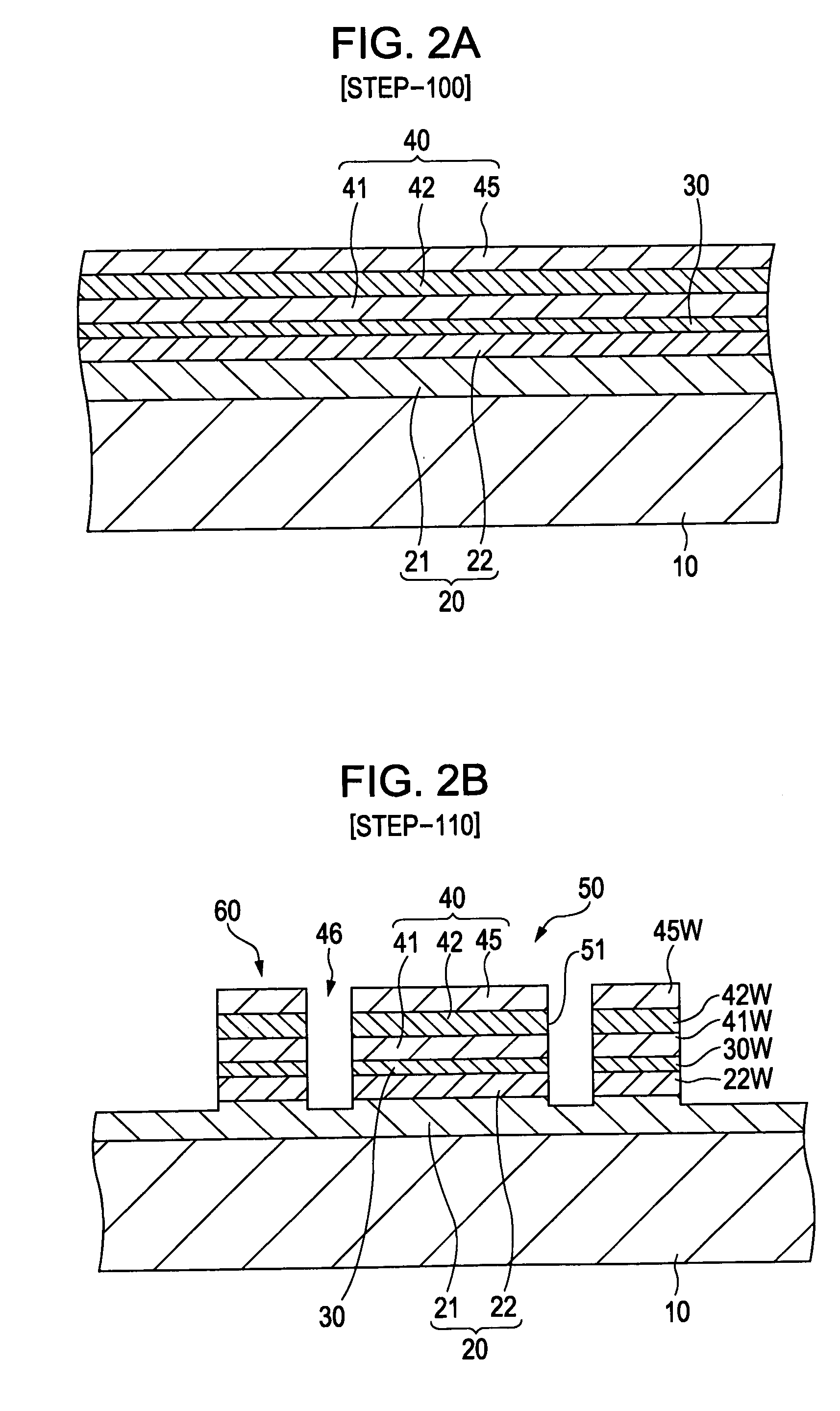
[0066]Example 1 relates to a light-emitting element according to the first embodiment of the present invention and a method for manufacturing the light-emitting element according to the first embodiment. FIGS. 1A and 1B are a schematic partial cross-sectional view and a schematic partial plan view, respectively, of a light-emitting element in Example 1. Note that in Example 1 or Example 2 or 3, which will be described later, the first conductivity type is n type, and the second conductivity type is p type. Furthermore, in Example 1 or Examples 2 or 3, which will be described later, the light-emitting element is a surface-emitting laser element (vertical cavity surface-emitting laser; VCSEL) in which light is emitted through a second compound semiconductor layer.

[0067]The light-emitting element of Example 1 has a mesa structure 50 in which a first compound semiconductor layer 20 of the first conductivity type (n type), an active layer 30, and a second compound semiconductor layer 40 ...

example 2

[0088]Example 2 relates to a light-emitting element according to the second embodiment of the present invention and a method for manufacturing the light-emitting element according to the second embodiment. FIGS. 8A and 8B are a schematic partial cross-sectional view and a schematic partial plan view, respectively, of a light-emitting element in Example 2.

[0089]As in Example 1, the light-emitting element of Example 2 has a mesa structure in which a first compound semiconductor layer 20 of the first conductivity type (n type), an active layer 30, and a second compound semiconductor layer 40 of the second conductivity type (p type) are disposed in that order. At least one of the first compound semiconductor layer 20 and the second compound semiconductor layer 40 has a current constriction region 44 surrounded by an insulation region 43 extending inward from a sidewall portion 51 of the mesa structure 50. Specifically, as in Example 1, the light-emitting element of Example 2 has the mes...

example 3

[0106]Example 3 relates to a light-emitting element according to the third embodiment of the present invention and a method for manufacturing the light-emitting element according to the third embodiment. FIGS. 13A and 13B are a schematic partial cross-sectional view and a schematic partial plan view, respectively, of a light-emitting element in Example 3.

[0107]As in Example 1, the light-emitting element of Example 3 has a mesa structure 50 in which a first compound semiconductor layer 20 of the first conductivity type (n type), an active layer 30, and a second compound semiconductor layer 40 of the second conductivity type (p type) are disposed in that order (specifically, disposed in that order on a substrate 10). At least one of the first compound semiconductor layer 20 and the second compound semiconductor layer 40 has a current constriction region 44 surrounded by an insulation region 43 extending inward from a sidewall portion 51 of the mesa structure 50. That is, the light-emi...


PUM


Abstract

A light-emitting element includes a mesa structure in which a first compound semiconductor layer of a first conductivity type, an active layer, and a second compound semiconductor layer of a second conductivity type are disposed in that order, wherein at least one of the first compound semiconductor layer and the second compound semiconductor layer has a current constriction region surrounded by an insulation region extending inward from a sidewall portion of the mesa structure; a wall structure disposed so as to surround the mesa structure; at least one bridge structure connecting the mesa structure and the wall structure, the wall structure and the bridge structure each having the same layer structure as the portion of the mesa structure in which the insulation region is provided; a first electrode; and a second electrode disposed on a top face of the wall structure.

Description

CROSS REFERENCES TO RELATED APPLICATIONS[0001]The present invention contains subject matter related to Japanese Patent Application JP 2007-109654 filed in the Japanese Patent Office on Apr. 18, 2007, the entire contents of which are incorporated herein by reference.BACKGROUND OF THE INVENTION[0002]1. Field of the Invention[0003]The present invention relates to a light-emitting element and a method for manufacturing the same.[0004]2. Description of the Related Art[0005]In a surface-emitting laser element, on a substrate, for example, an active layer having a multiple quantum well structure is disposed in a cavity sandwiched between two mirror layers provided on upper and lower sides thereof, light emitted from the active layer under current injection is confined, and thus laser oscillation is caused. In such a surface-emitting laser element, a cylindrical mesa structure is usually employed, for example, as disclosed in Japanese Unexamined Patent Application Publication No. 2005-02662...

Claims


Application Information

Patent Timeline
Patent Type & Authority Applications(United States)
IPC IPC(8): H01S5/18H01L21/02H01S5/323
CPCB82Y20/00H01S5/0425H01S5/18311H01S5/18338H01S5/3432H01S5/343H01S2301/18H01S5/125H01S5/18H01S5/22H01S2301/176H01S5/04252H01S5/04254H01S5/221H01S5/34313H01S5/2231H01S5/187H01S5/02251H01S5/02253H01S5/18308
Inventor OKI, TOMOYUKIMASUI, YUJIYAMAUCHI, YOSHINORIKODA, RINTAROARAKIDA, TAKAHIRO
Owner SONY CORP
Why Eureka
Try Eureka