Apparatus for ion beam fabrication

a technology of ion beams and apparatuses, applied in the direction of material analysis using wave/particle radiation, instruments, nuclear engineering, etc., can solve the problems of inability to compensate beams have grown seriously anomalous, and no compensation can be made by changing the scanning speed, etc., to achieve stable operation of apparatuses, improve the yield of semiconductor processes, and high reliability

Active Publication Date: 2008-11-20
HITACHI HIGH-TECH CORP
View PDF5 Cites 31 Cited by
  • Summary
  • Abstract
  • Description
  • Claims
  • Application Information

AI Technical Summary

Benefits of technology

[0013]The present invention enables to realize the stable operation of the apparatus for ion beam fabrication and to carry out highly reliable failure analyses, and contributes to improve yield of semiconductor processes. In particular, due to the presence of a blanker and a beam current detector on the ion source side of the aperture, it is possible to monitor the stability of the beam current itself irradiated on the aperture while limiting damages to the projection mask and the like that are plate members with an aperture, and therefore it is possible to grasp any anomalies on the ion source side from the aperture. In addition, due to the provision of the second blanker and the second beam current detector on the specimen side of the aperture, it is possible to monitor the detailed condition of the ion beams in cooperation with the first blanker and the first beam current detector, and to monitor the stability of ion beams used for processing of the apparatus for ion beam fabrication while restricting the damages on projection masks and the like that are plate members having an aperture.

Problems solved by technology

In the case of PJIB, however, since generally no scanning is made and only the mask shape is projected, it is impossible to compensate by changing the scanning speed.
And there are cases where beams have grown seriously anomalous and no compensation can be made by changing the scanning speed.
For example, if the beam has deviated from the center of optical axis by some circumstance, the beam profile itself has been broken, and the beam skirt grows large causing the processing shape to collapse.
And since ion beams cause damages to the constituent elements exposed to the irradiation of the beam in the optical system, this can implicate the service life of the constituent elements.
In this case also, it is impossible to compensate in the conventional cases mentioned above.
Since a projection mask has a function of selectively allowing the passage of only the ion beams used for processing specimens, the ion beams barred from passing through are damaged by the spattering of the projection mask itself.
However, thickening brings about a problem in that delicate patterns cannot be shaped because of the problem of processing aspect.
For example, when you want to form a 10 μm wide pattern on a mask, the adoption of a 1 mm thick mask will result in a processing aspect ratio of 100 and it will be difficult to make a mask.
Consequently, the thickness of mask due to the shaping pattern size is generally limited by an upper limit, which is for example approximately 300 μm.
In this case also, there is a problem of service life because, like the projection mask, the movable aperture diaphragm is spattered by illumination beam.
In this case, it is impossible to compensate the beam irradiation condition on a specimen by simply compensating the beam irradiation time as in the conventional case.
Particularly in the case of a FIB device used for miocrofabrication beam skirt leads fatally to processing failures, and it is important therefore to prevent it from being used under such anomalous conditions.

Method used


Image

  • Apparatus for ion beam fabrication
  • Apparatus for ion beam fabrication
  • Apparatus for ion beam fabrication

Examples


first embodiment

[0035]In the present embodiment, we will describe the configuration of the PJIB device according to the present invention.

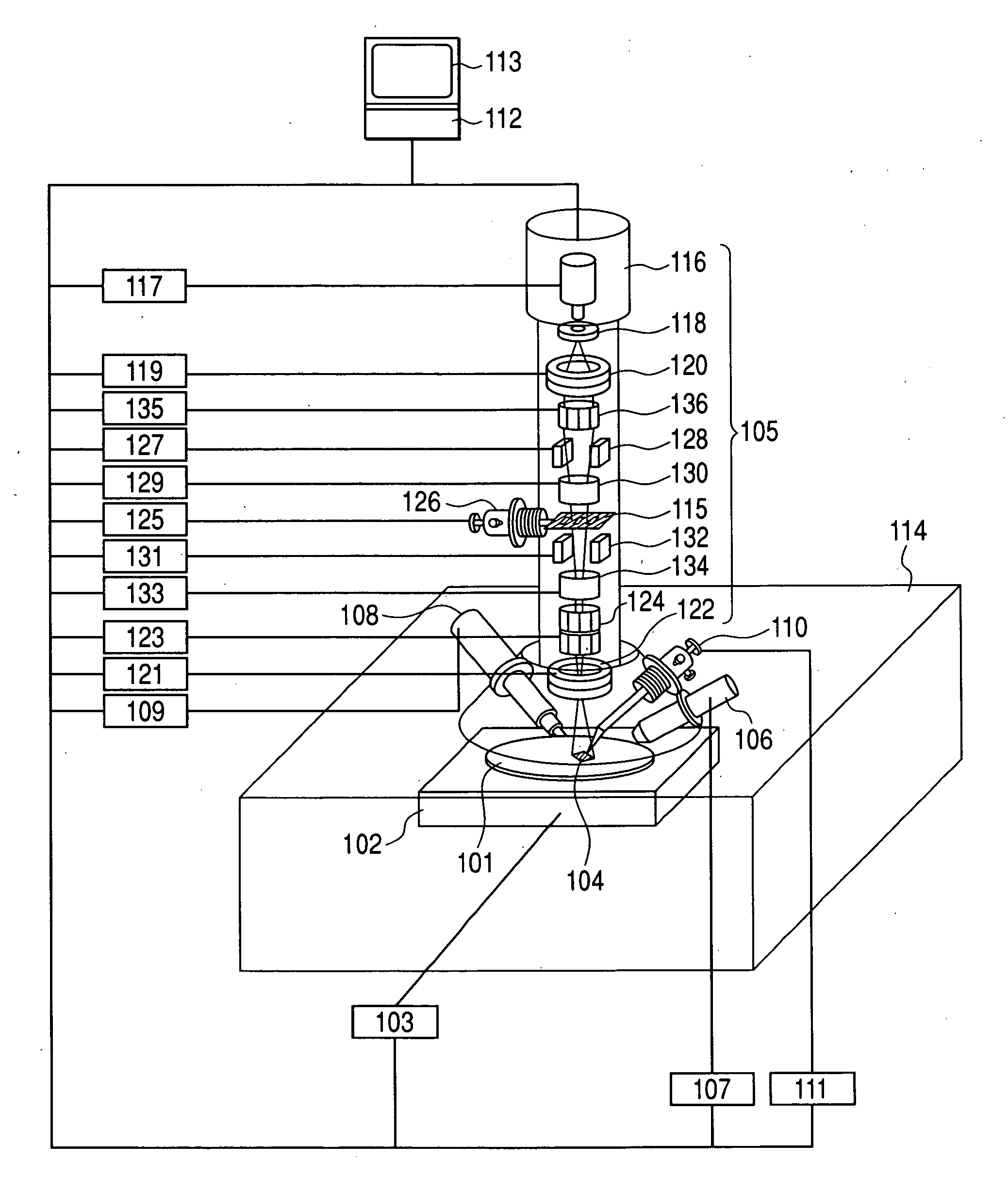
[0036]The PJIB device shown in FIG. 1 includes a movable specimen stage 102 for carrying the substrate of a specimen 101 such as a semiconductor wafer and the like, a specimen-stage position controller 103 for controlling the position of the specimen stage 102 for identifying the observation and processing position of the specimen 101, an ion-beam irradiating optical system 105 for processing the specimen 101 by irradiating the same with ion beams 104, and a secondary-electron detector 106 for detecting the secondary electrons emitted by the specimen 101. The secondary-electron detector 106 is controlled by a controller for secondary-electron detector 107. An assisting gas supplying source 108 for supplying the assist gas used for the ion beam assist deposition or the ion beam assist etching is controlled by a controller for assisting gas supplying source 109. An...

embodiment 2

[0075]In this embodiment, we will describe an apparatus for ion beam fabrication for realizing detailed control of the service life of the projection mask by the present invention.

[0076]As described in First Embodiment, the projection mask 115 is a part having a short service life among the constituent parts in the device. Accordingly, while the replacement of any mask on which a failure of ion beam current has been found as shown in FIG. 1 is a way to deal with the situation, the estimation of its service life followed by its replacement in good time is effective for preventing any processing failures and for assuring a stable operation. However, leaving too much margin leads to a problem in that its service life is reduced. For this reason, it is important to estimate as precisely as possible its service life. In First Embodiment we described the relationship between the illumination ion beam Ib2 and the specimen processing by means of Formula 4. The same principle applies to the ...

third embodiment

[0083]In this embodiment, we will describe a FIB device for detecting anomalies in ion beams according to the present invention.

[0084]In the First Embodiment and the Second Embodiment, we described the example of PJIB. However, similar detection of ion beam can be realized in the case of FIB also. The FIB device shown in FIG. 20 includes a movable specimen stage 2102 for placing the specimen substrate of a specimen 2101 such as semiconductor wafer and the like, a specimen-stage position controller 2103 for controlling the position of a specimen stage 2102 for specifying the observation and fabricating position of the specimen 2101, an ion-beam irradiating optical system 2105 for irradiating the specimen 2101 with ion beam 2104 and fabricating the same, and a secondary-electron detector 2106 for detecting the secondary electrons coming from the specimen 2101. The secondary-electron detector 2106 is controlled by a controller 2107 for secondary-electron detector. An assisting gas supp...


PUM


Abstract

The apparatus for ion beam fabrication, which has been able to detect any anomalous condition of ion beams only by means of the current irradiated on the specimen, could not compensate the failure by investigating the cause and could not realize stable processing. To solve the problem described above, the present invention includes the first and second blankers and Faraday cups switches ON and OFF the first and second blankers and monitors beam current at two positions above and below the projection mask. By adopting this configuration, it will be possible to acquire the information on failure in ion beam, sort out the cause of the failure and to compensate the failure while limiting damages to the projection mask. As a result, it will be possible to realize stable processing by means of ion beam, and to use the ion beam fabricating device on a stable basis.

Description

CLAIM OF PROPERTY[0001]The present application claims priority from Japanese application JP 2007-008063 filed on Jan. 17, 2007, the content of which is hereby incorporated by reference into this application.FIELD OF THE INVENTION[0002]The present invention relates to an apparatus for ion beam fabrication for manufacturing specimens used in tests and failure analyses of devices and the like.BACKGROUND OF THE INVENTION[0003]The needs are rising for tests and analyses of semiconductor devices that are becoming progressively minute. In failure analyses for specifying the cause of failure, in particular, the direct observation of defects within devices has become an indispensable technology. For these observations, it is necessary to precisely microfabricate the position of observation objects of the device. So far, this precise miocrofabrication has been carried out by means of a tool called “focused ion beam (hereinafter referred to as “FIB”) processing device.” As this FIB enables to ...

Claims


Application Information

Patent Timeline
Patent Type & Authority Applications(United States)
IPC IPC(8): H01J37/08
CPCH01J37/045H01J37/244H01J37/304H01J37/3056H01J2237/24405H01J2237/24507H01J2237/24535H01J2237/24542H01J2237/30472
Inventor TOMIMATSU, SATOSHISHICHI, HIROYASUKANEOKA, NORIYUKIUMEMURA, KAORUISHIGURO, KOJI
Owner HITACHI HIGH-TECH CORP
Why Eureka
Try Eureka