

RF shutter
- Summary
- Abstract
- Description
- Claims
- Application Information
AI Technical Summary
Benefits of technology
Problems solved by technology
Method used
Image

Examples
Embodiment Construction
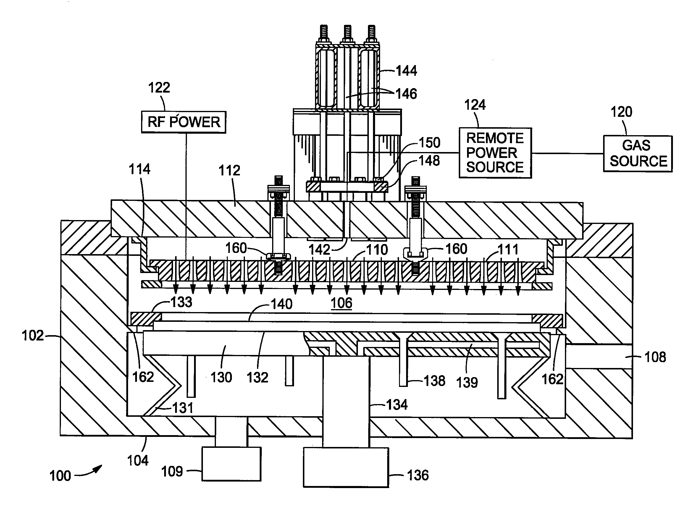
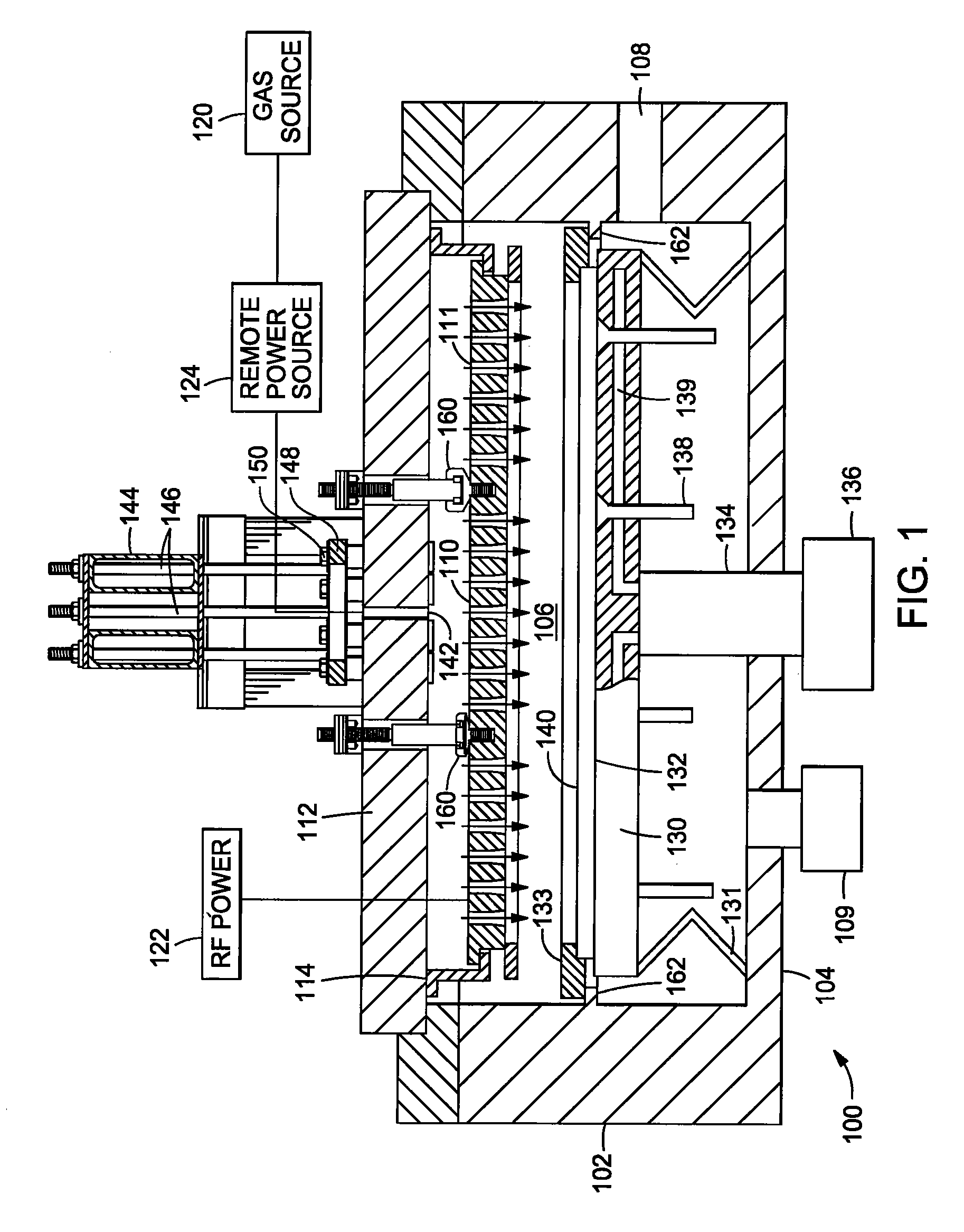
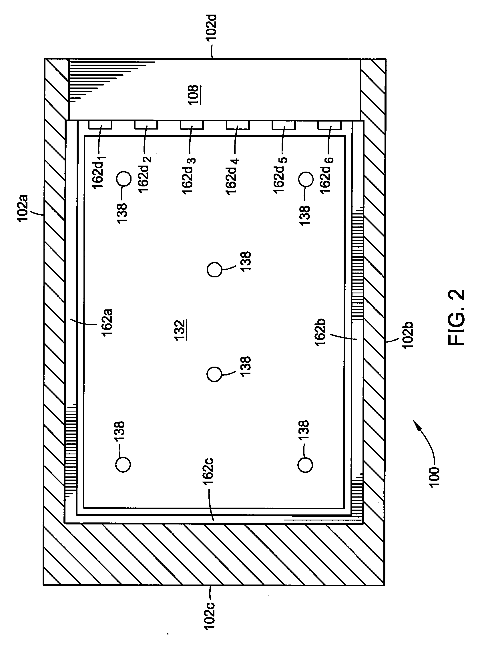
[0020]The present invention generally relates to an RF shutter assembly for use in a plasma processing apparatus. The RF shutter assembly may reduce the amount of plasma creep below the substrate and shadow frame during processing, thereby reducing the amount of deposition that occurs on undesired surfaces. By reducing the amount of deposition on undesired surfaces, particle flaking and thus, substrate contamination may be reduced.
[0021]FIG. 1 is a cross sectional view of a PECVD apparatus according to one embodiment of the invention. The apparatus includes a chamber 100 in which one or more films may be deposited onto a substrate 140. As shown in FIG. 1, the substrate is in a lowered position where processing may not occur. One suitable PECVD apparatus which may be used is available from AKT, a subsidiary of Applied Materials, Inc., located in Santa Clara, Calif. While the description below will be made in reference to a PECVD apparatus, it is to be understood that the invention is...
PUM
| Property | Measurement | Unit |
|---|---|---|
| Length | aaaaa | aaaaa |
Abstract
Description
Claims
Application Information