This may further result in additional space being available for the design-in of a larger display.
However, it is not necessary that the circuits are constructed of substantially transparent material, nor is application of the considered device limited to use with the described information display.
The result is that resistive and capacitive touchscreens, while simple in principle, are often difficult to manufacture, and which usually employ one of two very different methods to achieve the stated
linearity of the touch
system.
While some averaging and analog or digital filtering of multiple readings by the controller of the same touch location may occur, there is no non-linear or non-orthogonal mapping of the touch voltages to accurately describe the Cartesian space.
While this design criterion usually means that close attention to materials and design are critical, and that extensive testing of the finished
touchscreen may be required for
verification of the stated
linearity specification, it also means that such a
touchscreen is also not matched to a specific controller or external memory circuit (see second method) and requires no
linearization to achieve its stated
linearity specification.
Some impairment of speed of response is seen when used in
fast motion continuous touch applications.
Another consequence is that a third-party controller may not be designed to perform this same type of
linearization.
While the
touchscreen and this
third party controller may function adequately together for some applications, the linearity of the touch
system is likely to suffer near the edges, and particularly in the corners of the touchscreen.
Such linearity problems will be especially noticeable in applications where
graphical user interface (GUI) “desktops” are controlled with the touchscreen rather than application programs designed for touch control.
These GUI desktops typically have small targets, in the corners of the display, that must be touched to start or stop application programs or the computer itself A further consequence is that the NVRAM
chip must be programmed at the factory, with increased expense for the manufacturer, or by the customer, which increases the opportunities for mistakes in performing the
linearization.
Further, elements of
material selection and touchscreen design can have a significant affect on service life and durability.
As a result, the quality and the manufacturing cost of touchscreens are adversely affected.
(i) Uncontrollable uniformity and stability of resistance.
However, the inked area of the
conductive ink layer is typically less than 50% of the print area due to the size of meshes of the screen when the
conductive ink (e.g.,
silver paste) is printed on the transparent resistive layer.
As a result, an uneven surface is formed at every position on the printed circuits.
Moreover, it is difficult to control thickness uniformity and registration of the circuits due to ink
viscosity, squeegee pressure and blade sharpness, snap-off distance, and other parameters well known to those skilled in the art of
screen printing.
This is particularly inappropriate for products having a very high accuracy requirement with respect to line spacing and edge quality.
As a result, touch panels manufactured by the prior
screen printing cannot meet the demand of quality.
(ii) Poor adhesion to the surface of conductive glass.
Such circuits are too soft to withstand other parts of the manufacturing process.
Subsequent
exposure of the finished product to
moisture may further degrade the adhesion of the silver-resistive film interface, resulting in deterioration of the linearity of the touchscreen.
(iv) Difficulties in further
processing and uncontrollable quality.
Whether the conductive ink is UV curable or thermosetting, difficulties in maintaining the consistency of the screen printed ink are well known to those skilled in the art.
Further, because the ink is expensive, and disposal is complicated by considerations of
hazardous waste, there is always a goal of recycling unused ink.
Manufacturer's recommendations about the proper capturing and reconstituting of the unused ink are vague, and lead to uncertain quality and consistency of traces printed with recycled ink.
While there are many novel and reliable
interconnection systems for specific applications, the general use of these systems to interconnect conductive ink circuits to other circuits, such as cables and first sheet to second sheet
electrical contacts, is not as reliable as
soldering.
While it is possible to design drive traces that have equal resistance from the external cable attachment point to the connection point of the
peripheral circuit
proximate the edge of the resistive sheet, the manufacturing process may not yield the same resistance for each drive trace.
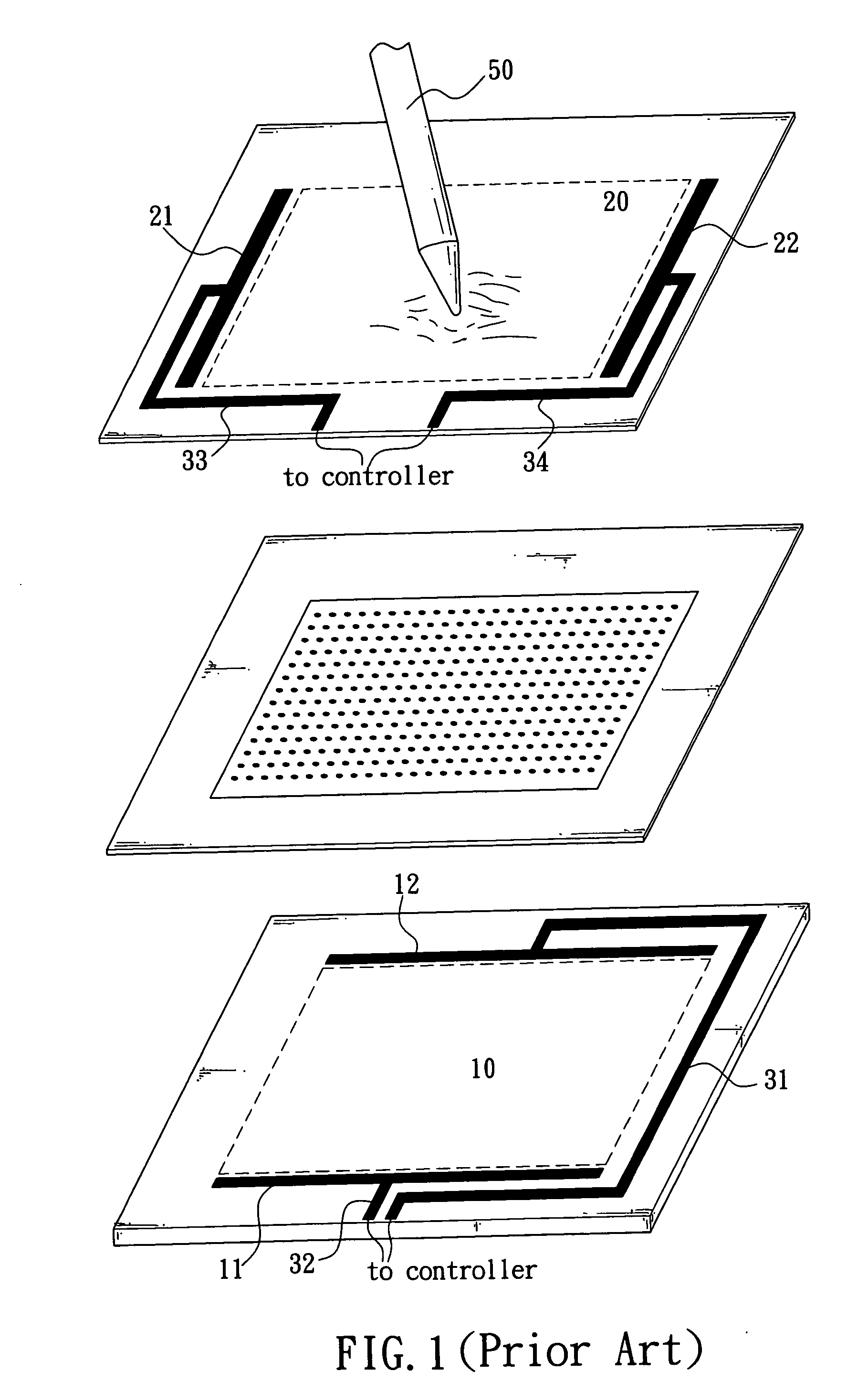
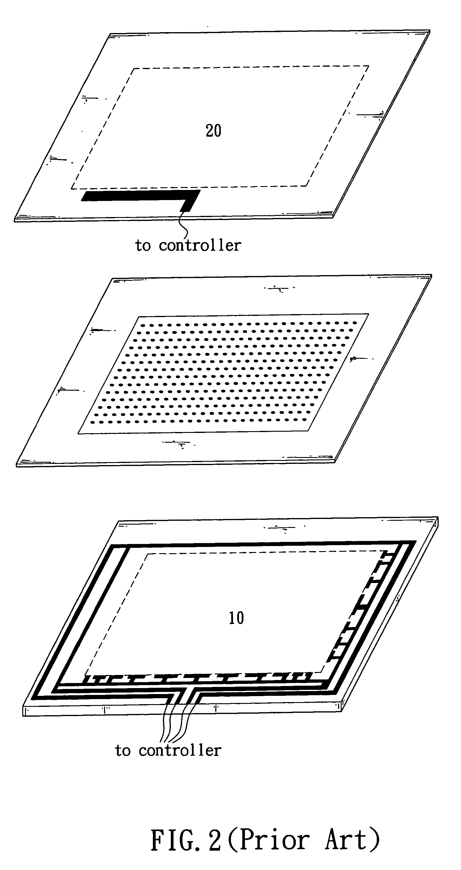
In a 5-wire touchscreen, unequal drive trace resistances will cause a non-linearity of the touchscreen.
This will cause a non-linearity in the touchscreen.
Again a non-linearity of the touchscreen will result.
While it is possible to increase the design width of the
bus bar perpendicular to the direction of current flow on the resistive sheet in anticipation of this problem, the mechanical size of the touchscreen may be increased unacceptably.
Poor consistency in the resistivity of the elements of the
peripheral circuit and poor adhesion of the elements to the resistive film will result in non-uniform current flow and touchscreen non-linearity.
While the results of this process can be of good quality, adhesion and
hardness, the firing process temperatures also affect the resistivity of the resistive film surrounding the silver
frit.
Thus the design of the silver
frit pattern must be adjusted to compensate for the changes in resistivity of the
frit, introducing various uncertainties in the design that ultimately affect the linearity of the touchscreen.

