

Method forming epitaxial silicon structure
a technology of epitaxial silicon and structure, which is applied in the direction of semiconductor/solid-state device details, electrical equipment, basic electric elements, etc., can solve the problems of affecting the overall reliability of the semiconductor device, affecting the heat budget of the device being manufactured, and posing potential problems to the process designer, so as to improve the epitaxial silicon structure and reduce defects
- Summary
- Abstract
- Description
- Claims
- Application Information
AI Technical Summary
Benefits of technology
Problems solved by technology
Method used
Image

Examples
Embodiment Construction
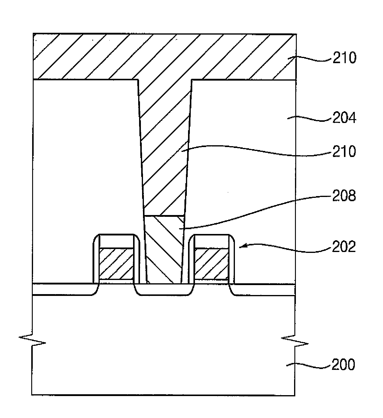
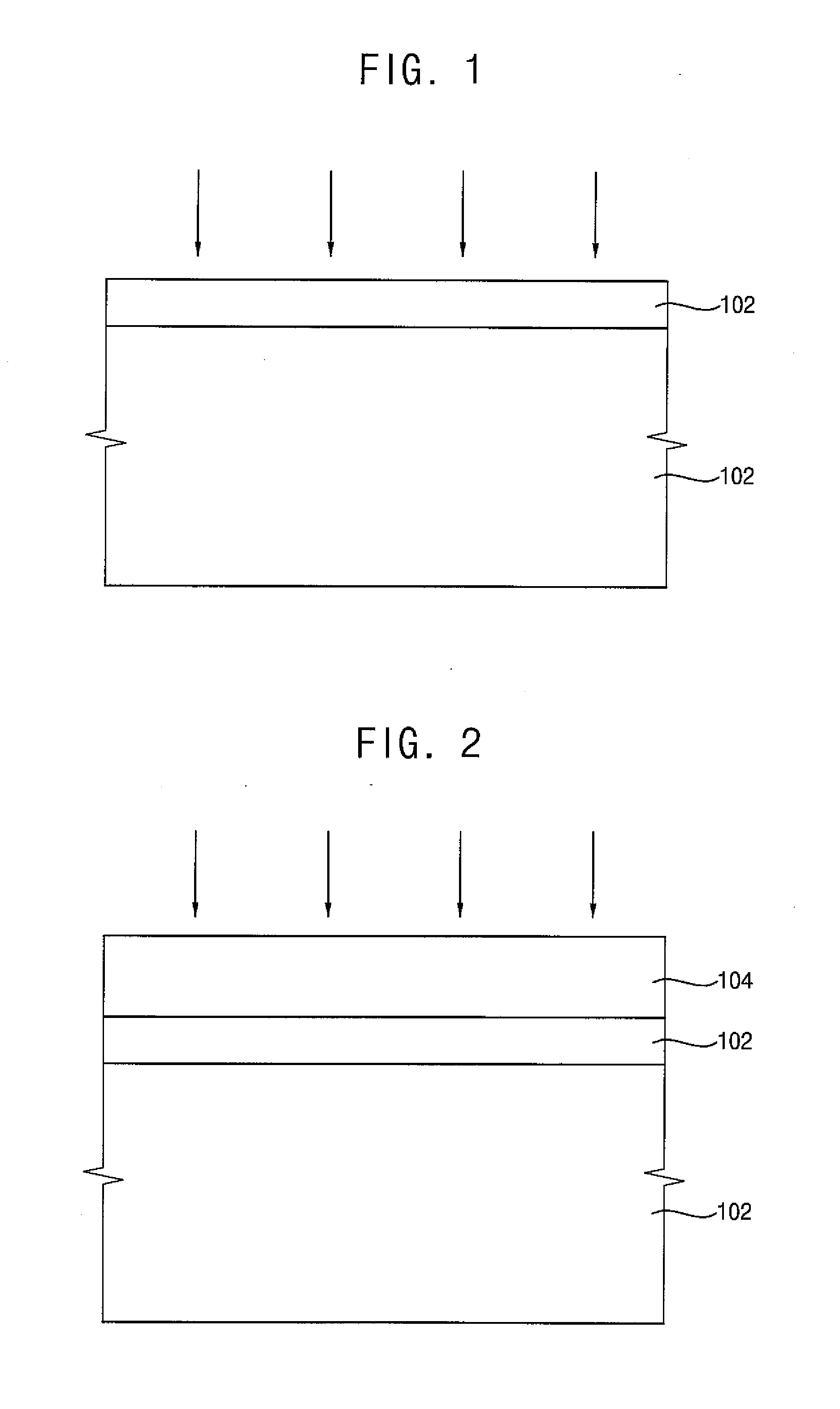
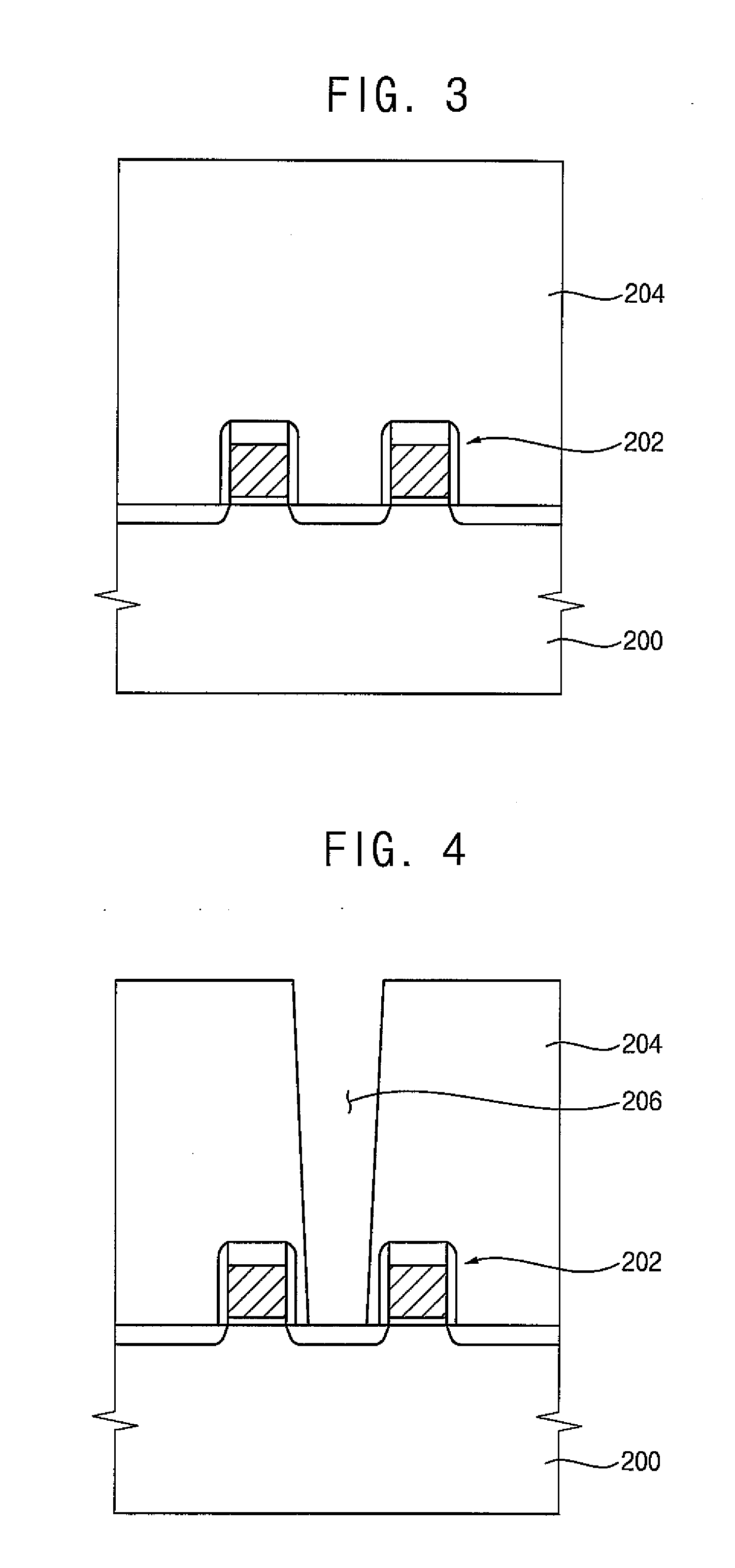
[0015]Several embodiments of the invention will be described with reference to the accompanying drawings. The present invention may, however, be embodied in many different forms and should not be construed as being limited to only the illustrated embodiments. Rather, these example embodiments are provided as teaching examples. In the drawings, the size and / or relative size of various layers and / or regions may be exaggerated for clarity. Throughout the drawings and written description, like reference numerals refer to like or similar elements.
[0016]It will be understood that when an element or layer is referred to as being “on,”“connected to” or “coupled to” another element or layer, it can be directly on, connected or coupled to the other element or layer or intervening elements or layers may be present. In contrast, when an element is referred to as being “directly on,”“directly connected to” or “directly coupled to” another element or layer, there are no intervening elements or la...
PUM
| Property | Measurement | Unit |
|---|---|---|
| temperature | aaaaa | aaaaa |
| temperature | aaaaa | aaaaa |
| temperature | aaaaa | aaaaa |
Abstract
Description
Claims
Application Information