Current/voltage mode image sensor with switchless active pixels

a switchless, image sensor technology, applied in the direction of color television details, television system details, television systems, etc., can solve the problems of low pixel sensitivity, high dark current and high temporal noise, and the introduction of extra switch transistors, so as to reduce the size (pitch) of the pixel, improve the resolution of the image sensor, and improve the effect of pixel sensitivity

Active Publication Date: 2008-11-27
THE TRUSTEES OF THE UNIV OF PENNSYLVANIA
View PDF6 Cites 32 Cited by
  • Summary
  • Abstract
  • Description
  • Claims
  • Application Information

AI Technical Summary

Benefits of technology

[0008]The present invention relates to an imaging sensor based on the linear current mode APS paradigm in which the pixel addressing (switch) transistor has been moved outside the pixel, thus allowing for an efficient realization of two transistors per pixel and effectively reducing the size (pitch) of the pixel. Furthermore, eliminating the switch transistor from the pixel has allowed for higher linearity between the output photo current and photodiode voltage. The improved linearity has a direct influence on the spatial variations across the sensor and therefore a lowering of the FPN figures.

Problems solved by technology

One of the drawbacks of the 3T APS are high dark currents and high temporal noise.
Unfortunately, the introduction of the extra switch transistor comes at a cost of larger pixel size and a lowering of the resolution of the image sensor.
Both pixel topologies rely on capacitive addressing of the pixel resulting in low pixel sensitivity and increased spatial variations due to the increased capacitance at the photodiode node.
However, large spatial variations, such as high fixed pattern noise, caused by gain variations of the in-pixel BJT, were one of the drawbacks of this implementation.
Unfortunately, the shallow photodiode and high parasitic capacitance associated with intra-tier connections have had a direct impact on the poor sensitivity of the image sensor.
The limiting factor in such current mode imaging sensors has been the low image quality due to the large fixed pattern noise (see Table 2).
The primary contributor of fixed pattern noise in both voltage and current mode APS is the threshold voltage variations of the read-out transistor between pixels in the imaging array.
Due to the non-linear relationship between light and output current noted by Delbruck et al. versus Boussaid et al, canceling out voltage threshold variations is not easily performed on a chip.
However, one of the factors which has limited the linearity of the current output (hence impacting the FPN figure) has been the finite on-resistance of the access transistor in the pixel.

Method used


Image

  • Current/voltage mode image sensor with switchless active pixels
  • Current/voltage mode image sensor with switchless active pixels
  • Current/voltage mode image sensor with switchless active pixels

Examples


Embodiment Construction

[0027]Certain specific details are set forth in the following description with respect to FIGS. 1-11 to provide a thorough understanding of various embodiments of the invention. Certain well-known details are not set forth in the following disclosure, however, to avoid unnecessarily obscuring the various embodiments of the invention. Those of ordinary skill in the relevant art will understand that they can practice other embodiments of the invention without one or more of the details described below. Also, while various methods are described with reference to steps and sequences in the following disclosure, the description is intended to provide a clear implementation of embodiments of the invention, and the steps and sequences of steps should not be taken as required to practice the invention.

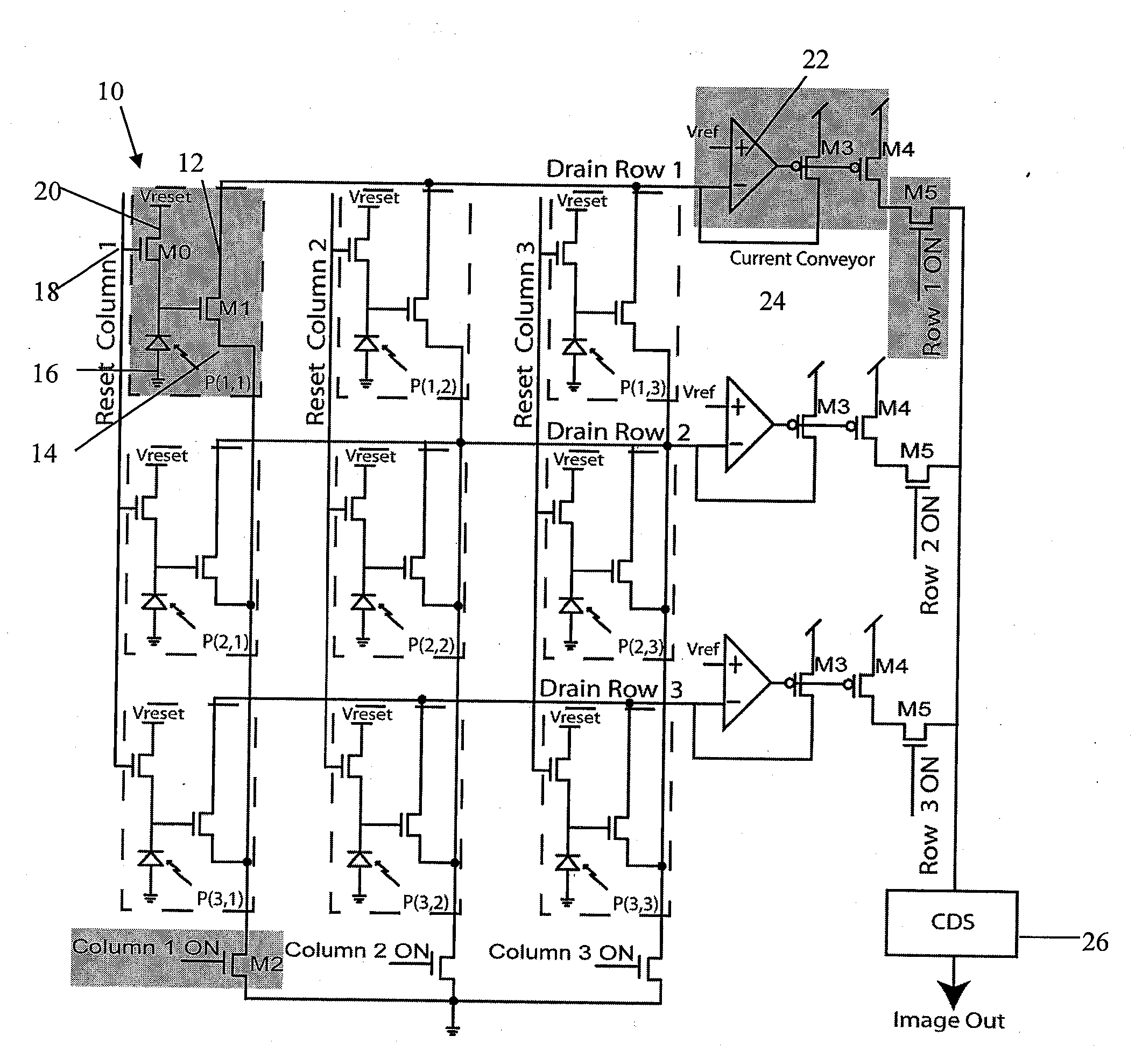
[0028]A block diagram of the pixel schematic for an exemplary embodiment of a two transistors per pixel linear current mode CMOS imager is presented in FIG. 1. The photo pixel 10 comprises a p...


PUM


Abstract

A voltage and current mode active pixel sensor for high resolution imaging is presented. The photo pixel is composed of a photodiode and two transistors: reset and transconductance amplifier transistor. The switch transistor is moved outside the pixel, allowing for lower pixel pitch and increased linearity of the output photocurrent. The reset and amplifier (readout) transistors may also be shared among adjacent pixels by the introduction of transfer switches between the photodiodes and the source of the reset transistor and the gate of the readout transistor. The switch transistor outside the pixels provides biasing voltages or currents to the readout transistors to selectively turn them on when readout of the corresponding photodiode is desired and turns the readout transistor off when the corresponding photodiode is not to be read out. The increased linearity of the image sensor has greatly reduced spatial variations across the image after correlated double sampling and the column fix pattern noise is greatly improved.

Description

GOVERNMENT SUPPORT[0001]The present invention was supported by the U.S. Air Force Office of Scientific Research (AFOSR) under Grant Number FA9550-05-1-0052. The government may have certain rights in the invention.FIELD OF THE INVENTION[0002]The present invention relates to a current / voltage mode active pixel sensor architecture in which the pixel sensor is composed of 1.5 or 2.0 transistors per pixel, thus allowing for higher resolution and more pixels per given area of silicon.BACKGROUND OF THE INVENTION[0003]High resolution imaging is closely related to the number of transistors and interconnections per pixel. Traditional voltage mode image sensors have been based on the three transistor (3T) active pixel sensor (APS) topology which has been coined by E. R. Fossum in “CMOS Image Sensor: Electronic Camera-On-A-Chip,” IEEE Trans. Electron Devices, Vol. 44, pp. 1689-1698, October 1997. The three transistor topology, which has been widely accepted as the industry standard, is composed...

Claims


Application Information

Patent Timeline
Patent Type & Authority Applications(United States)
IPC IPC(8): H04N5/335H04N5/365H04N5/376
CPCH04N5/3658H04N5/3741H04N5/37457H04N5/378H04N25/677H04N25/766H04N25/778H04N25/75
Inventor GRUEV, VIKTORYANG, ZHENGVAN DER SPIEGEL, JAN
Owner THE TRUSTEES OF THE UNIV OF PENNSYLVANIA
Why Eureka
Try Eureka