
Thin film transistor, array substrate and method for manufacturing the same

a thin film transistor and array substrate technology, applied in the field of thin film transistors, can solve the problems of imposing a high requirement on the magnitude of the charging current and cannot meet the demand for a higher charging current, so as to improve the display quality without decreasing the aperture ratio of the pixel region, increase the charging current (ion), and reduce failur

Active Publication Date: 2008-12-04
BEIJING BOE OPTOELECTRONCIS TECH CO LTD +1
View PDF15 Cites 7 Cited by
  • Summary
  • Abstract
  • Description
  • Claims
  • Application Information

AI Technical Summary

Benefits of technology

[0008]In view of the above problems in the related art, the objects of the present invention are to provide a thin film transistor for a TFT-LCD to increase the charging current (Ion), decrease the failure due to the insufficient charging, and improve the display quality without decreasing the aperture ratio of the pixel region.
[0012]Compared with the conventional technology, the embodiments of the present invention increase the charging current of the pixel region of the TFT by extending the channel and increase the ration of the width to length of the channel (W / L) without decreasing the aperture ratio. The display failures such as bright spot and gray level non-uniformity are efficiently avoided.

Problems solved by technology

With rapid spread and wide application of thin film transistor liquid crystal displays (TFT-LCDs), there is an increasing demand for a larger display screen, and thus pixels for display are also becoming larger, which in turn imposes a high requirement on the magnitude of the charging current.
However, the conventional charging channel structure may lead to many failures due to the insufficient charging current and thus cannot satisfy the demand for a higher charging current of a TFT-LCD.

Method used


Image

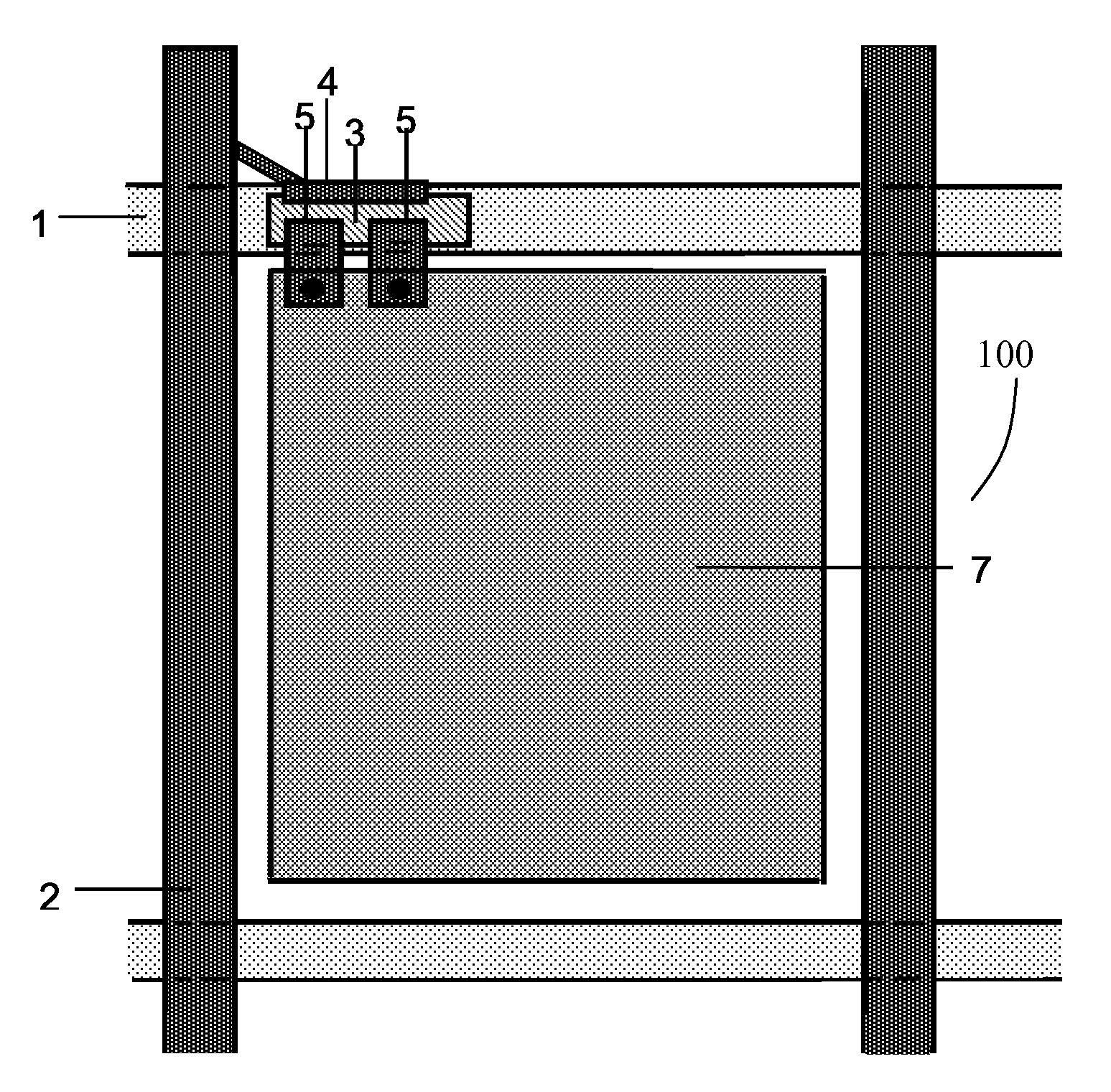
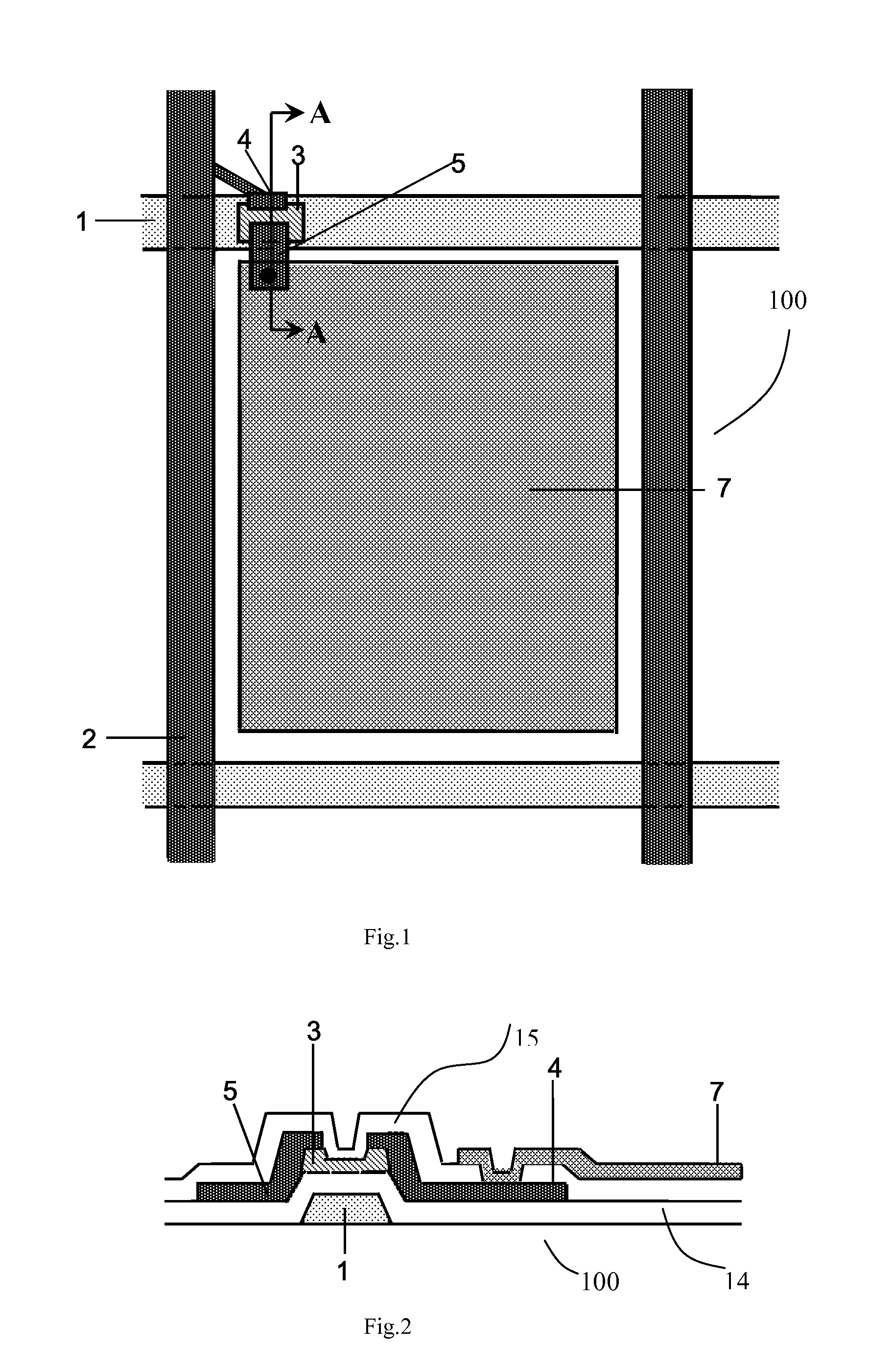
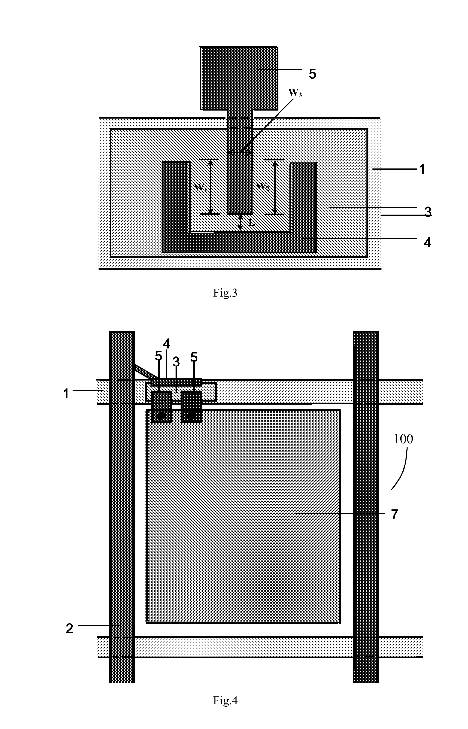
  • Thin film transistor, array substrate and method for manufacturing the same
  • Thin film transistor, array substrate and method for manufacturing the same
  • Thin film transistor, array substrate and method for manufacturing the same

Examples


embodiment 1

[0024]FIG. 7 is a diagram of a TFT-LCD channel structure according to a first embodiment of the present invention. As shown in FIG. 7, the TFT channel structure comprises a source 5, a drain 4, a U-type channel region, and a channel extension region (between a source extension region 10 and a drain extension region 11). The source extension region 10 and the source 5 vertically intersect with each other and form an integrated structure together. The drain 4 is a U-type drain. The drain extension region 11 is formed at both ends of the U-type drain 4 and forms an integrated structure with the drain 4. The channel extension region is formed between the source extension region 10 and the drain extension region 11 and extends at both sides of the U-type channel formed between the source 5 and the U-type drain 4. The extension region comprises the same metal material as that used for the signal line and the source and drain electrode, such as a material selected from the group consisting...

embodiment 2

[0029]FIG. 8 is a diagram of a TFT-LCD channel structure with a single source and a single drain according to a second embodiment of the present invention. As shown in FIG. 8, the TFT channel structure comprises a source 5, a drain 4, a U-type channel region and a channel extension region (between a source extension region 10 and a drain extension region 11). The source extension region 10 and the source 5 vertically intersect with each other and form an integrated structure together. Here, the drain 4 is a U-type drain. The drain extension region 11 is formed at both sides of the U-type drain 4 and forms an integrated structure with the drain 4. The above structure is the same as that in embodiment 1, and the difference between embodiment 2 and embodiment 1 lies in that the source extension region 10 and the drain extension region 11 are disposed opposite to each other in the form of a zigzag or corrugation shape. Because the length between the source extension region 10 and the dr...


PUM


Abstract

A thin film transistor for a thin film transistor liquid crystal display (TFT-LCD), an array substrate and manufacturing method thereof are provided. The thin film transistor comprises a source, a drain, and a channel region between the source and drain. A source extension region is connected with the source, a drain expanded region is connected with the drain, and the source extension region is disposed opposite to the drain extension region to form a channel extension region therebetween.

Description

FIELD OF THE INVENTION[0001]The present invention relates to a thin film transistor for a liquid crystal display (LCD), an array substrate and a method of manufacturing the same.BACKGROUND OF THE INVENTION[0002]With rapid spread and wide application of thin film transistor liquid crystal displays (TFT-LCDs), there is an increasing demand for a larger display screen, and thus pixels for display are also becoming larger, which in turn imposes a high requirement on the magnitude of the charging current. How to improve the charging current of the pixels has become critical in the technology.[0003]A typical TFT-LCD comprises a TFT array substrate and a color filter substrate arranged in parallel to each other. Spacers are interposed between the two substrates to provide a space for filling liquid crystal therein. On the TFT array substrate, gate lines and data lines (signal lines) that intersect with each other to define pixels, and at the intersection between a gate line and a data line...

Claims


Application Information

Patent Timeline
Patent Type & Authority Applications(United States)
IPC IPC(8): H01L29/786H01L21/336
CPCH01L29/41733H01L29/66765
Inventor LI, XINXINWANG, WEILONG, CHUNPING
Owner BEIJING BOE OPTOELECTRONCIS TECH CO LTD
Learn More