Integrated circuit structures with multiple FinFETs

a technology of integrated circuits and fins, applied in the field of semiconductor devices, can solve the problems of increasing gate width, circuit failure, and conflicting with the requirements of reducing the size of semiconductor devices, and achieve the effect of reducing the problem of un-removed photoresist and reducing the residue of gate electrodes

Active Publication Date: 2008-12-04
ADVANCED MFG INNOVATIONS INC
View PDF15 Cites 126 Cited by
  • Summary
  • Abstract
  • Description
  • Claims
  • Application Information

AI Technical Summary

Benefits of technology

[0012]By reducing the fin space between fins of the neighboring FinFETs, the gate electrode residue problem resulted from the un-removed photoresist is reduced, and possibly eliminated.

Problems solved by technology

The increase in gate widths, however, conflicts with the requirements of reducing sizes of semiconductor devices.
As a result, the gates of the resulting FinFETs may be shorted, causing circuit failure.

Method used


Image

  • Integrated circuit structures with multiple FinFETs
  • Integrated circuit structures with multiple FinFETs
  • Integrated circuit structures with multiple FinFETs

Examples


Embodiment Construction

[0017]The making and using of the presently preferred embodiments are discussed in detail below. It should be appreciated, however, that the present invention provides many applicable inventive concepts that can be embodied in a wide variety of specific contexts. The specific embodiments discussed are merely illustrative of specific ways to make and use the invention, and do not limit the scope of the invention.

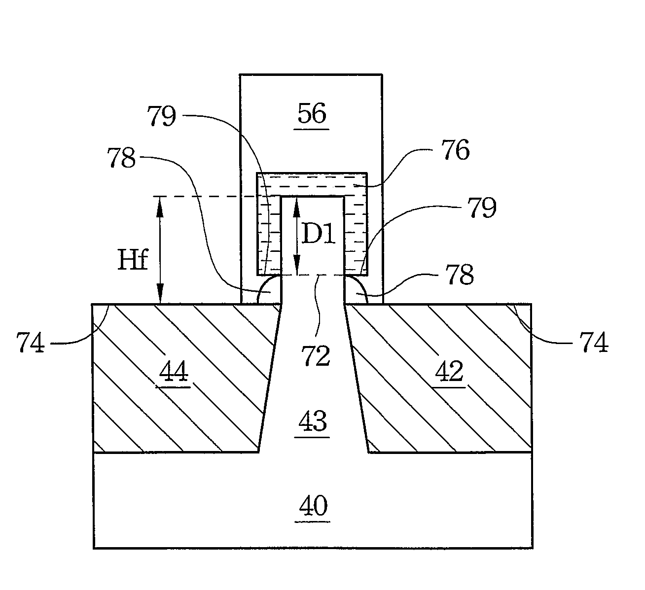
[0018]FIG. 4A illustrates a perspective view of an intermediate stage in the formation of an embodiment of the present invention. A portion of substrate 40 is illustrated. Preferably, substrate 40 comprises bulk silicon. Alternatively, substrate 40 comprises bulk SiGe or other semiconductor materials. Shallow trench isolation (STI) regions 42 and 44 are formed on substrate 40 to isolate device regions. As is known in the art, STI regions 42 and 44 may be formed by etching substrate 40 to form recesses, and then filling the recesses with dielectric materials, such as high-dens...


PUM


Abstract

A semiconductor structure includes a semiconductor substrate; and a first Fin field-effect transistor (FinFET) and a second FinFET at a surface of the semiconductor substrate. The first FinFET includes a first fin; and a first gate electrode over a top surface and sidewalls of the first fin. The second FinFET includes a second fin spaced apart from the first fin by a fin space; and a second gate electrode over a top surface and sidewalls of the second fin. The second gate electrode is electrically disconnected from the first gate electrode. The first and the second gate electrodes have a gate height greater than about one half of the fin space.

Description

TECHNICAL FIELD[0001]This invention relates generally to semiconductor devices, and particularly to structures and formation methods of Fin field-effect transistors (FinFET).BACKGROUND[0002]Transistors are key components of modern integrated circuits. To satisfy the requirements of increasingly faster speed, the drive currents of transistors need to be increasingly greater. Since the drive currents of transistors are proportional to gate widths of the transistors, transistors with greater widths are preferred.[0003]The increase in gate widths, however, conflicts with the requirements of reducing sizes of semiconductor devices. Fin field-effect transistors (FinFET) are thus formed. FIG. 1 illustrates a perspective view of a conventional FinFET. Fin 4 is formed as a vertical silicon fin extending above substrate 2, and is used to form source and drain regions 6 and a channel region therebetween (not shown). A vertical gate 8 intersects the channel region of fin 4. While not shown in F...

Claims


Application Information

Patent Timeline
Patent Type & Authority Applications(United States)
IPC IPC(8): H01L29/76
CPCH01L21/823431H01L21/823437H01L21/845H01L27/088H01L27/1211H01L29/165H01L29/41791H01L29/66795H01L29/7843H01L29/7848H01L29/785H01L29/7851
Inventor LEE, TSUNG-LINCHANG, CHANG-YUNLIU, SHENG-DAYANG, FU-LIANG
Owner ADVANCED MFG INNOVATIONS INC
Why Eureka
Try Eureka