Supercharge Your Innovation With Domain-Expert AI Agents!

Gapfill extension of hdp-cvd integrated process modulation sio2 process

a technology of integrated process and process, applied in the direction of coating, chemical vapor deposition coating, metallic material coating process, etc., can solve the problems of increasing the aspect ratio, progressively more difficult to fill gaps without leaving voids, and reducing the width of gaps

Inactive Publication Date: 2008-12-04
APPLIED MATERIALS INC
View PDF19 Cites 7 Cited by
  • Summary
  • Abstract
  • Description
  • Claims
  • Application Information

AI Technical Summary

Benefits of technology

The invention provides methods for depositing a silicon oxide film on a substrate with a gap between raised surfaces. The method involves using a high-density plasma made of a silicon-containing gas, an oxygen-containing gas, and a fluent gas to deposit the silicon oxide film. The deposition rate is between 900 and 60000 Å / min with a deposition / sputter ratio greater than 20. The method also involves etching a portion of the deposited film using a halogen-containing gas and then depositing a second portion of the film over the etched film. The second portion is deposited using a second high-density plasma made of a silicon-containing gas, an oxygen-containing gas, and a fluent gas. The method can be used to deposit silicon oxide films with a thickness between 300 and 1000 Å.

Problems solved by technology

One of the persistent challenges faced in the development of semiconductor technology is the desire to increase the density of circuit elements and interconnections on substrates without introducing spurious interactions between them.
As circuit densities increase, however, the widths of these gaps decrease, increasing their aspect ratios and making it progressively more difficult to fill the gaps without leaving voids.
The formation of voids when the gap is not filled completely is undesirable because they may adversely affect operation of the completed device, such as by trapping impurities within the insulative material.
The high reactivity of the species in the plasma reduces the energy required for a chemical reaction to take place, and thus lowers the temperature required for such CVD processes when compared with conventional thermal CVD processes.
Semiconductor manufacturers have discovered, however, that there is a practical limit to the aspect ratio of gaps that HDP-CVD processes are able to fill.
It has been reported that when such a process is used to fill certain narrow-width high-aspect-ratio gaps, the sputtering caused by argon in the process gas may hamper the gapfill efforts.
This, in turn, may result in the formation of a void in the gap if the upper areas of regrowth join before the gap is completely filled.

Method used


Image

  • Gapfill extension of hdp-cvd integrated process modulation sio2 process
  • Gapfill extension of hdp-cvd integrated process modulation sio2 process
  • Gapfill extension of hdp-cvd integrated process modulation sio2 process

Examples


Embodiment Construction

[0020]Embodiments of the invention are directed to methods of depositing a silicon oxide layer to fill a gap in a surface of a substrate using a high-density-plasma CVD process. Silicon oxide films deposited according to the techniques of the invention have excellent gapfill capabilities and are able to fill gaps encountered in, for example, shallow-trench-isolation (“STI”) structures. Films deposited by the methods of the invention are thus suitable for use in the fabrication of a variety of integrated circuits, including those that have a feature size on the order of or less than 45 nm.

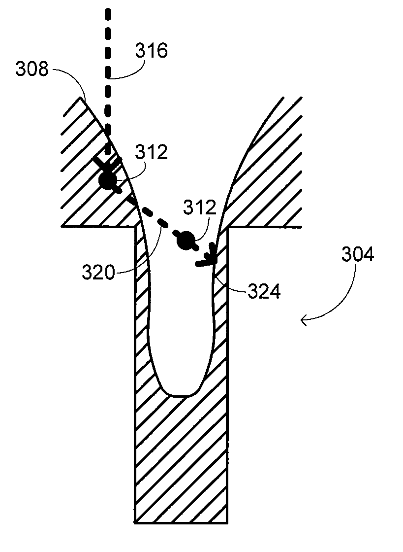
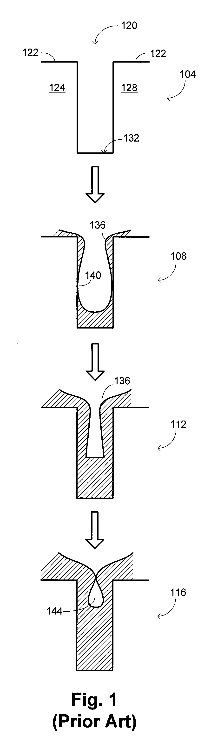
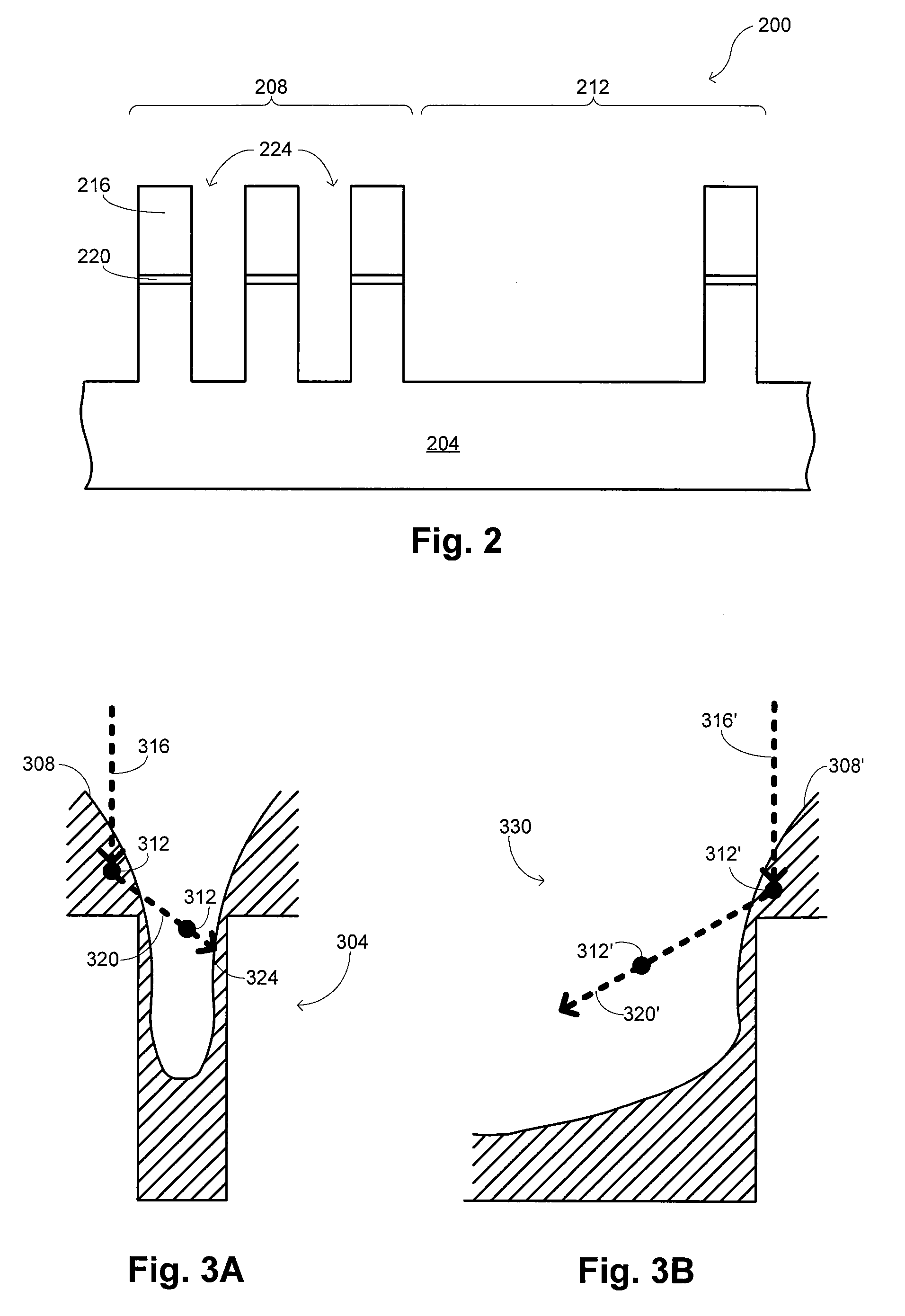
[0021]The types of structures that may be filled according to embodiments of the invention are illustrated by FIG. 2, which provides a simplified cross-sectional view of a partially completed integrated circuit 200. This integrated circuit is formed over a substrate 204 that includes a plurality of STI structures, each of which is typically created by forming a thin pad oxide layer 220 over the surf...


PUM

PropertyMeasurementUnit
feature sizeaaaaaaaaaa
temperatureaaaaaaaaaa

Abstract

Methods are disclosed for depositing a silicon oxide film on a substrate disposed in a substrate processing chamber. The substrate has a gap formed between adjacent raised surfaces. A silicon-containing gas, an oxygen-containing gas, and a fluent gas are flowed into the substrate processing chamber. A high-density plasma is formed from the silicon-containing gas, the oxygen-containing gas, and the fluent gas. A first portion of the silicon oxide film is deposited using the high-density plasma at a deposition rate between 900 and 6000 Å / min and with a deposition / sputter ratio greater than 30. The deposition / sputter ratio is defined as a ratio of a net deposition rate and a blanket sputtering rate to the blanket sputtering rate. Thereafter, a portion of the deposited first portion of the silicon oxide film is etched. A second portion of the silicon oxide film is deposited over the etched portion of the silicon oxide film.

Description

BACKGROUND OF THE INVENTION[0001]One of the persistent challenges faced in the development of semiconductor technology is the desire to increase the density of circuit elements and interconnections on substrates without introducing spurious interactions between them. Unwanted interactions are typically prevented by providing gaps or trenches that are filled with electrically insulative material to isolate the elements both physically and electrically. As circuit densities increase, however, the widths of these gaps decrease, increasing their aspect ratios and making it progressively more difficult to fill the gaps without leaving voids. The formation of voids when the gap is not filled completely is undesirable because they may adversely affect operation of the completed device, such as by trapping impurities within the insulative material.[0002]Common techniques that are used in such gapfill applications are chemical-vapor deposition (“CVD”) techniques. Conventional thermal CVD pro...

Claims


Application Information

Patent Timeline
Patent Type & Authority Applications(United States)
IPC IPC(8): H01L21/311
CPCC23C16/045C23C16/45523C23C16/507H01L21/02164H01L21/02274H01L21/31116H01L21/31608H01L21/76229H01L21/31H01L21/469
Inventor WANG, ANCHUANLEE, YOUNG S.VELLAIKAL, MANOJBLOKING, JASON THOMASJEON, JIN HOMUNGEKAR, HEMANT P.
Owner APPLIED MATERIALS INC
Features
  • R&D
  • Intellectual Property
  • Life Sciences
  • Materials
  • Tech Scout
  • Unparalleled Data Quality
  • Higher Quality Content
  • 60% Fewer Hallucinations
Learn More