Multilayer printed wiring boards with holes requiring copper wrap plate

a multi-layer printing and copper wrap plate technology, applied in the direction of resistive material coating, lithographic masks, etching metal masks, etc., can solve the problems of circuit board failure, the thickness of wraparound plating does not completely eliminate the occurrence of circuit board failures, and the heat dissipation of more hea

Active Publication Date: 2008-12-11
TTM TECH NORTH AMERICA LLC
View PDF8 Cites 32 Cited by
  • Summary
  • Abstract
  • Description
  • Claims
  • Application Information

AI Technical Summary

Benefits of technology

[0014]Aspects of embodiments of the present invention are directed toward methods, systems and/or apparatus (1) to enhance the consistency of the wraparound plating of holes of printed circuit boards with (requiring) via fill...

Problems solved by technology

In addition, the conductive ink filled holes are more conductive to electrical signals and also dissipate more heat than non-filled holes.
However, reliability problems may still occur with these printed circuit boards having the ink filled holes.
These reliability problems typically occur during the component assembly process of the printed circuit boards because this is when the printed circuit boards are exposed to a series of thermal heat excursions.
However, the wraparound plating thickness does not completely eliminate the occurrences of circuit board failures, such as surface conductor separation from h...

Method used


Image

  • Multilayer printed wiring boards with holes requiring copper wrap plate
  • Multilayer printed wiring boards with holes requiring copper wrap plate
  • Multilayer printed wiring boards with holes requiring copper wrap plate

Examples


Embodiment Construction

[0056]In the following detailed description, only certain exemplary embodiments of the present invention have been shown and described, simply by way of illustration. As those skilled in the art would realize, the described embodiments may be modified in various different ways, all without departing from the spirit or scope of the present invention. Accordingly, the drawings and description are to be regarded as illustrative in nature and not restrictive.

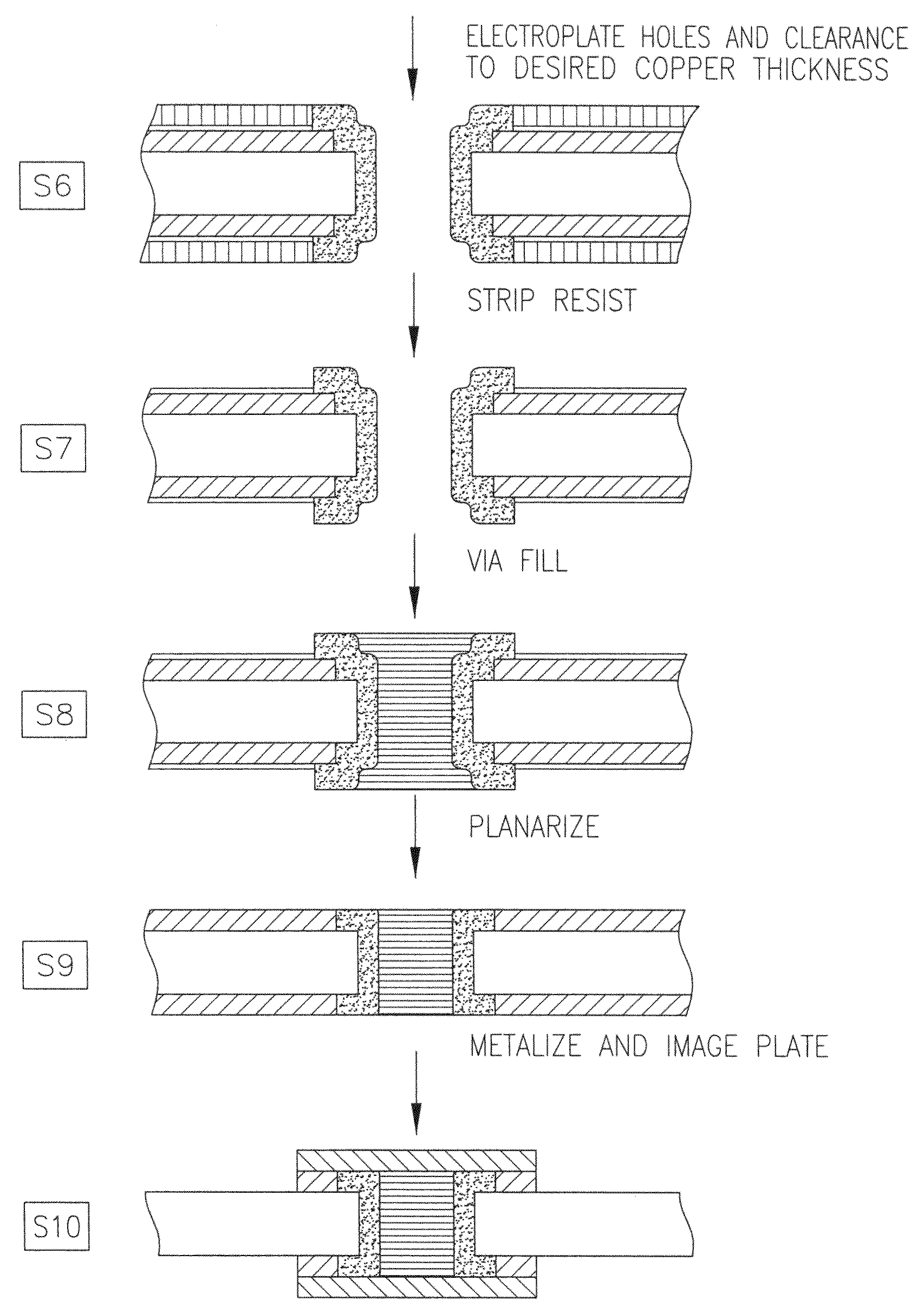
[0057]In the context of the present invention, holes refer to through-, blind-, buried-, and / or micro-vias and / or holes. In addition, metalization, metalize, and / or metalizing refer to electroless copper (or electroless coppering) or alternate Metalizing process using, e.g., Shadow process (Electrochemicals, Inc.), Eclipse Process (McDermid, Inc.), Dylex process (Okuno Chemical), etc.

[0058]Here, holes are drilled and plated with copper to the minimum required hole wall thickness in the printed circuit boards to connect copper patter...


PUM

PropertyMeasurementUnit
Thicknessaaaaaaaaaa
Sizeaaaaaaaaaa
Electrical conductoraaaaaaaaaa

Abstract

Printed circuit boards have circuit layers with one or more via filled holes with copper wraps and methods of manufacturing the same. An embodiment of the present invention provides a method to enhance the consistency of the wraparound plating of through-hole vias of printed circuit boards with (requiring) via filling to provide extra reliability to the printed circuit boards and enables the designers and/or manufacturers of printed circuit boards to design and manufacture boards with relatively fine features and/or tight geometries.

Description

CROSS-REFERENCE TO RELATED APPLICATION(S)[0001]This application claims priority to and the benefit of U.S. Provisional Application No. 60 / 933,541, filed on Jun. 6, 2007, the entire content of which is incorporated herein by reference.BACKGROUND OF THE INVENTION[0002]1. Field of the Invention[0003]The present invention relates to multilayer printed wiring boards with holes requiring copper wrap plates and methods of manufacturing the same.[0004]2. Description of the Related Art[0005]Most electronic systems include printed wiring (or circuit) boards with high density electronic interconnections. A printed circuit board may include one or more circuit cores, substrates, or carriers. In one fabrication scheme for the printed circuit board having the one or more circuit carriers, electronic circuitries (e.g., pads, electronic interconnects, patterns, etc.) are fabricated onto opposite sides of an individual circuit carrier to form a pair of circuit layers. These circuit layer pairs of th...

Claims


Application Information

Patent Timeline
IPC IPC(8): H05K3/46
CPCH05K1/116H05K3/243H05K3/427H05K3/4602H05K2201/0347H05K2201/0959Y10T29/49128H05K2203/0554H05K2203/1476Y10T29/49155Y10T29/49156Y10T29/49165H05K2203/025
Inventor SIDHU, RAJWANT SINGH
Owner TTM TECH NORTH AMERICA LLC
Why Eureka
Try Eureka