High voltage and high power boost conveter with co-packaged schottky diode

a high-power boost and conveter technology, which is applied in the direction of dc-dc conversion, apparatus without intermediate ac conversion, solid-state devices, etc., can solve the problems of limiting the active area of components that can be included in a given package, unable to meet the power (current) or voltage requirement, and the production cost of such devices tends to be high. , to achieve the effect of small form factor and low manufacturing cos

Active Publication Date: 2008-12-11
ALPHA & OMEGA SEMICON LTD
View PDF13 Cites 26 Cited by
  • Summary
  • Abstract
  • Description
  • Claims
  • Application Information

AI Technical Summary

Benefits of technology

[0017]The anode 208 of the discrete Schottky diode 203 may be bonded directly to the drain D of the NFET 205 on the IC, or to the common package pin at junction J. The bottom cathode 210 may be directly coupled to the output voltage VOUT. The source S of the discrete NFET 205 may be directly coupled to ground. An external inductor L may be directly coupled between the input voltage VIN and drain D of the discrete NFET 205. A capacitor C may be coupled between the bottom cathode 210 of the vertical discrete Schottky diode 203 and ground. An output voltage VOUT may be obtained at a point between the cathode 210 of the Schottky diode 203 and the capacitor C. The boost converter IC 207 and the discrete Schottky diode 203 may be co-packaged on a common die pad 202, such as a standard single die pad lead frame, which may be electrically connected to the bottom cathode 210 of the discrete Schottky diode 203. The die pad 202 can be held at the output voltage VOUT as a result of the bonding. Since the output voltage VOUT is free of any large signal switching waveforms, the noise injected into the Boost IC substrate of the die pad 202 will be minimal.
[0020]The co-packaged configuration of the boost converter IC 207 and the discrete Schottky diode 203 on a common die pad 202 as shown in FIGS. 2A-2D provides the advantages of both low cost of manufacturing and small form factor.

Problems solved by technology

A small form factor for the total solution is needed as PCB space is always limited.
Unfortunately, most integrated Schottky diodes available in commercial IC processes do not have the area efficiency required to meet either the Power (Current) or Voltage requirement.
However, although the Schottky diode may be co-packaged with the IC, such a boost converter requires two die pads, one for the IC and one for the diode, which limits the active area of the components that can be included in a given package.
In addition, production costs for such devices tend to be high due to the assembly complexity and the cost of the lead frame for the two die pads.

Method used


Image

  • High voltage and high power boost conveter with co-packaged schottky diode
  • High voltage and high power boost conveter with co-packaged schottky diode
  • High voltage and high power boost conveter with co-packaged schottky diode

Examples


Embodiment Construction

[0015]Although the following detailed description contains many specific details for the purposes of illustration, anyone of ordinary skill in the art will appreciate that many variations and alterations to the following details are within the scope of the invention. Accordingly, the exemplary embodiments of the invention described below are set forth without any loss of generality to, and without imposing limitations upon, the claimed invention.

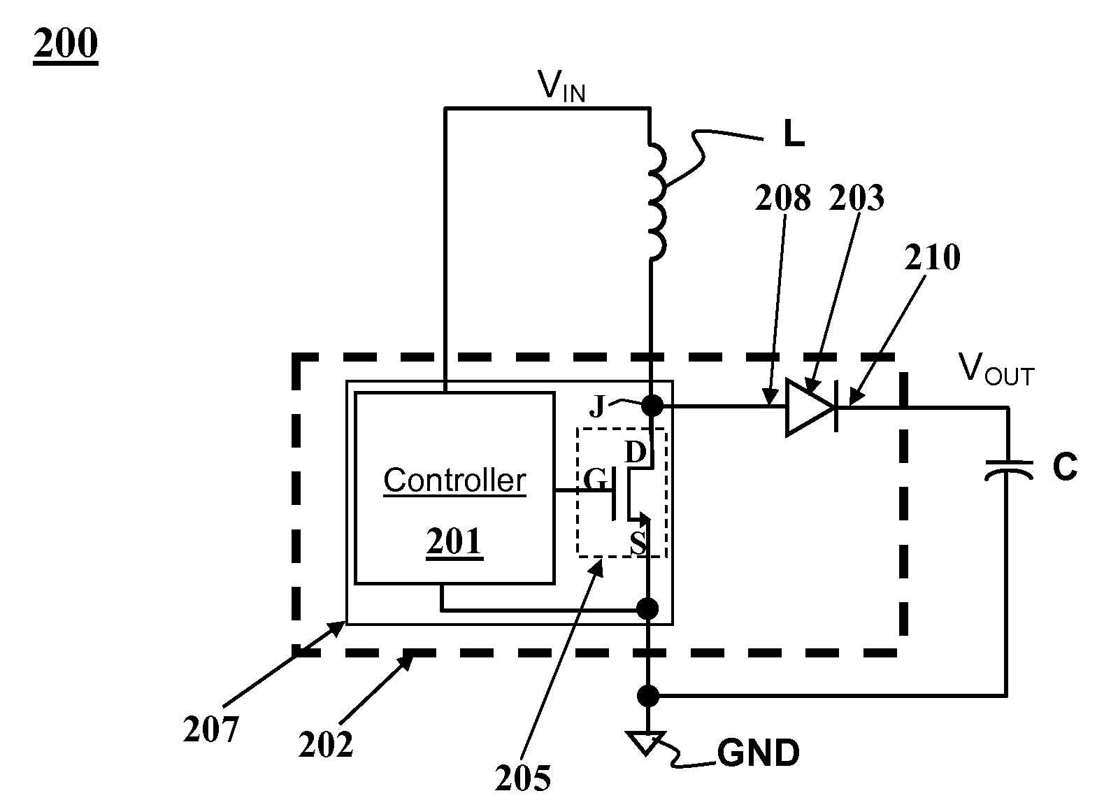
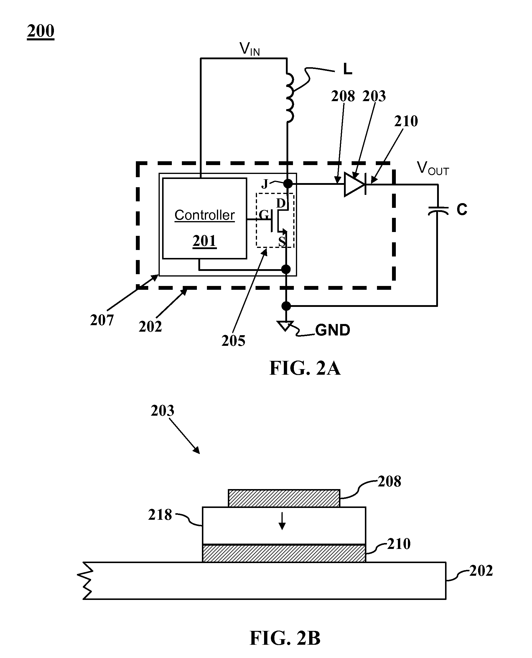
[0016]FIG. 2A is a circuit diagram illustrating a boost converter 200 according to a preferred embodiment of the present invention. As shown in FIG. 2A, boost converter 200 includes a boost converter IC 207 attached to and electrically insulated from a die pad 202 and a vertical discrete Schottky diode 203 attached to and electrically connected from the same die pad 202. The boost converter IC may include a controller 201 and a high voltage N-type field effect transistor (NFET) 205 with a source S, a drain D and a gate G. The controller 201 ...


PUM


Abstract

A high voltage and high power boost converter is disclosed. The boost converter includes a boost converter IC and a discrete Schottky diode, both of which are co-packaged on a standard single common die pad.

Description

CROSS-REFERENCE TO RELATED APPLICATIONS[0001]This application is related to co-pending application Ser. No. ______, to Allen Chang and Wai-Keung Peter Cheng, entitled “BOOST CONVERTER WITH INTEGRATED HIGH POWER DISCRETE FET AND LOW VOLTAGE CONTROLLER”, (Attorney Docket ANO-003 / US) filed on the same day as the present application, the entire disclosures of which are incorporated herein by reference.FIELD OF THE INVENTION[0002]This invention generally relates to boost converters and more particularly to high voltage and high power Boost converters having a co-packaged Schottky diode.BACKGROUND OF THE INVENTION[0003]Boost converter circuit is used to boost an input voltage to a higher output voltage. A boost ratio of ten or more is possible, e.g., in portable display applications. A boost converter may be used, e.g., to power a string of white LED diode for LCD backlight. In such situations boost converter may be used to convert a five volt input to an output voltage of up to 50V. A bo...

Claims


Application Information

Patent Timeline
Patent Type & Authority Applications(United States)
IPC IPC(8): H02M3/02H02M1/00
CPCH01L25/16H02M3/155H01L2924/12032H01L2224/49171H01L2224/32245H01L2224/73265H01L2224/48247H01L2924/13091H02M7/003H01L2924/00
Inventor CHANG, ALLENCHENG, WAI-KEUNG PETER
Owner ALPHA & OMEGA SEMICON LTD
Why Eureka
Try Eureka